Product overview of STM32F103VEH6
STM32F103VEH6 is a high‑density 32‑bit microcontroller based on the Arm Cortex‑M3 core, running up to 72 MHz and delivering approximately 1.25 DMIPS/MHz at zero wait‑state Flash access. It integrates 512 Kbytes of embedded Flash memory and up to 64 Kbytes of SRAM, placing it in the STM32F103xE performance line.
The device offers up to 112 fast I/O ports (in the high‑pin‑count package family), 3× 12‑bit ADCs with up to 21 channels total, 2× 12‑bit DAC channels, and up to 11 timers. Connectivity resources include CAN 2.0B active, USB 2.0 full speed device, SDIO, up to 5 USARTs, up to 3 SPIs (2 of them with I2S), and up to 2 I2C interfaces, alongside IrDA, LIN and ISO 7816 capabilities in certain USARTs.
STM32F103VEH6 operates over a 2.0 V to 3.6 V supply range and an ambient temperature from −40 °C to +85 °C. It provides several low‑power modes (Sleep, Stop, Standby), a real‑time clock domain powered from VBAT, on‑chip power supervision, and an internal voltage regulator.
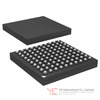
The device is packaged in a 100‑ball LFBGA (100‑LFBGA) form factor within the broader STM32F103 high‑density family that also spans LQFP64, LQFP100, LQFP144, LFBGA100, LFBGA144 and WLCSP64 options. STM32F103VEH6 is RoHS3 compliant, with MSL 3 (168‑hour floor life) classification and is listed as an active product.
2.
Core architecture and memory subsystem of STM32F103VEH6
STM32F103VEH6 centers on an Arm 32‑bit Cortex‑M3 CPU providing a balance of performance and code efficiency for embedded control. Operating up to 72 MHz, the core supports single‑cycle multiplication and hardware division, reducing execution time for arithmetic‑intensive tasks such as motor‑control algorithms, digital filtering or protocol handling.
The memory subsystem in STM32F103VEH6 includes:
- 512 Kbytes of embedded Flash memory for program and non‑volatile data storage.
- Up to 64 Kbytes of embedded SRAM for data and stack.
The Flash is designed for zero‑wait‑state operation at the top frequency under specified conditions, helping sustain the advertised Dhrystone performance. Flash endurance and retention are characterized in the family datasheet, enabling assessment of firmware update cycles and long‑term storage behavior.
In addition to core memories, STM32F103VEH6 integrates:
- A CRC calculation unit, enabling hardware‑assisted cyclic redundancy checks for code integrity verification and data communication robustness. This can be used, for example, during boot to validate a firmware image stored in the 512 Kbytes Flash, or in runtime to verify data blocks retrieved from external memories.
- A flexible static memory controller (FSMC) that links the internal bus matrix to external memories, extending addressable space for code or data and offloading timing management.
The nested vectored interrupt controller (NVIC) and the memory map are structured to deliver deterministic interrupt handling and efficient access to peripherals and SRAM. The 24‑bit SysTick timer, memory‑mapped in the core space, allows straightforward OS tick generation or periodic scheduling.
3.
Clocking, reset and power management in STM32F103VEH6
Reliable system design with STM32F103VEH6 depends strongly on its clock, reset, and power configuration.
Clocking architecture
STM32F103VEH6 includes:
- 4–16 MHz high‑speed external (HSE) crystal/clock input.
- 8 MHz internal high‑speed RC oscillator (HSI), factory trimmed.
- 32.768 kHz low‑speed external (LSE) oscillator dedicated to RTC.
- Internal 40 kHz low‑speed RC (LSI) oscillator.
- Phase‑locked loop (PLL) for frequency multiplication to 72 MHz core clock.
The clock tree enables flexible distribution of clock sources to the CPU, AHB, APB1, APB2 and peripherals. For example, a typical configuration might use an 8 MHz HSE crystal, feed it into the PLL, and multiply to 72 MHz for the core; APB1 can then be prescaled (e.g., to 36 MHz) to meet timing requirements of certain peripherals, while APB2 can run at full speed.
Reset and power supervision
The device implements:
- Power‑on reset (POR) and power‑down reset (PDR) circuits.
- A programmable voltage detector (PVD) to monitor VDD and generate interrupts or resets when supply drops below set thresholds.
This allows appropriate handling of brown‑out conditions and controlled system restart. The NRST pin characteristics and recommended external protection network are specified for robust reset line design.
Voltage regulator and supply
STM32F103VEH6 is powered from a 2.0 V to 3.6 V main supply and includes:
- An internal voltage regulator supplying the core from VDD.
- VBAT pin to supply the RTC and backup registers independently from the main supply.
Power supply decoupling, maximum pin input voltage ranges, and power supply schemes are detailed in the electrical characteristics. Typical application circuits show recommended decoupling and crystal connections.
Low‑power modes
STM32F103VEH6 offers three primary low‑power modes:
- Sleep: CPU clock stopped; peripherals remain clocked as configured.
- Stop: main regulator in run or low‑power mode, clocks stopped, SRAM and registers retained, fast wake‑up.
- Standby: lowest consumption; contents of SRAM lost, backup domain (RTC, backup registers) maintained from VBAT.
Typical and maximum current consumption figures are provided for each mode, across voltage and temperature ranges, together with wake‑up timings. For example, a battery‑powered data logger could run the core periodically from Flash at 72 MHz, then switch to Stop or Standby between measurements, using the RTC as a wake‑up source from VBAT.
4.
STM32F103VEH6 timers, motor control and watchdog resources
Timing and control functions are one of the most prominent features in STM32F103VEH6, with up to 11 timers available.
General‑purpose and basic timers
The device integrates:
- Up to four 16‑bit general‑purpose timers, each supporting up to four input capture/output compare channels, PWM generation, pulse counter and quadrature encoder input.
- Two 16‑bit basic timers designed to drive the DAC or generate periodic interrupts, without input capture capabilities.
These timers can be used for tasks such as precise PWM generation for power conversion, input frequency measurement, and multi‑channel timing events.
Motor‑control and advanced timers
STM32F103VEH6 includes:
- 2 × 16‑bit motor control PWM timers with dead‑time insertion and emergency stop functionality.
These are suited to three‑phase motor drives, where complementary PWM outputs and programmable dead‑time avoid shoot‑through in power stages. Hardware emergency stop inputs can immediately disable outputs in case of fault conditions detected elsewhere in the system.
Watchdog timers and SysTick
Robust operation is supported by:
- Independent watchdog (IWDG) driven from its own clock source, typically used for last‑resort recovery.
- Window watchdog (WWDG), allowing software supervision within a defined time window, useful in detecting software runaway or timing anomalies.
- A 24‑bit SysTick down‑counter, integrated in the Cortex‑M3 core, typically used for operating system tick and periodic tasks.
Timer electrical characteristics (resolution, maximum frequency, input capture and output compare timings) are documented to aid in selecting prescalers and auto‑reload values for required frequencies.
5.
STM32F103VEH6 communication interfaces and connectivity options
STM32F103VEH6 provides a broad range of on‑chip communication interfaces suitable for industrial, consumer, and automotive‑adjacent designs.
I2C interfaces
Up to 2 × I2C interfaces support standard modes compatible with SMBus/PMBus operation. Characteristics such as maximum SCL frequency, timing requirements and voltage levels are specified. A common usage is connecting EEPROMs, power‑management controllers, temperature sensors or other low‑speed peripherals.
USARTs
Up to 5 USARTs are available, each offering:
- Asynchronous UART mode.
- Synchronous mode.
- LIN support.
- IrDA capability.
- ISO 7816 smart‑card interface in some instances.
- Modem control features.
This range covers applications such as RS‑232/RS‑485 conversion, serial bootloaders, smart card readers, and IrDA‑based short‑range links.
SPI and I2S
STM32F103VEH6 integrates:
- Up to 3 × SPI interfaces, up to 18 Mbit/s.
- 2 of these SPI units support I2S (Inter‑IC Sound) mode.
SPI links are used to interface external serial Flash, high‑speed ADCs or sensor clusters, while I2S mode enables straightforward audio streaming to codecs or digital audio amplifiers.
CAN interface
A CAN 2.0B Active controller is on‑chip, facilitating use in networks that employ CAN for field communication. Electrical and timing characteristics are documented, allowing calculation of bit timing registers to fit a given bus speed and topology.
USB 2.0 full speed
The integrated USB 2.0 full‑speed device interface allows STM32F103VEH6 to appear as a USB peripheral (e.g., virtual COM port, mass storage, HID) in host systems. Startup time and DC characteristics, along with full‑speed signaling parameters, are specified for compliance with the USB standard.
SDIO interface
The SDIO interface supports SD/MMC cards, enabling external removable storage. Timing diagrams show standard and high‑speed SD modes. Firmware can use this interface to implement file systems for data logging or firmware update storage.
Together, these interfaces allow STM32F103VEH6 to act as a communication hub in systems that require bridging between legacy serial, USB, CAN and memory card domains.
6.
STM32F103VEH6 analog subsystem: ADC, DAC and temperature sensor
STM32F103VEH6 features a comprehensive analog subsystem well suited to measurement and control applications.
ADC subsystem
The device integrates:
- 3 × 12‑bit ADCs, total of up to 21 input channels.
- Conversion range from 0 to 3.6 V.
- Typical conversion time of 1 µs.
- Triple sample‑and‑hold capability, enabling multi‑channel synchronous sampling.
Detailed ADC characteristics include:
- Maximum conversion rate as a function of ADC clock frequency.
- Input impedance limits (RAIN max vs fADC).
- Accuracy specifications over reference conditions: offset error, gain error, integral and differential non‑linearity.
A typical use case is a multi‑phase power monitor where each ADC simultaneously samples phase currents and voltages through appropriate scaling networks, using the triple sample‑and‑hold mechanism for synchronized measurements.
DAC subsystem
STM32F103VEH6 includes:
- 2 × 12‑bit DAC channels with buffered and non‑buffered modes.
These can generate analog control voltages, reference signals, or audio‑range waveforms. Electrical specifications cover output range, settling time, output buffer drive capability and linearity.
Temperature sensor
An internal temperature sensor is connected to the ADC, providing a way to:
- Monitor die temperature for thermal management or system diagnostics.
Characteristics such as output voltage vs temperature and measurement accuracy are given. An embedded system may periodically sample this sensor to adjust CPU speed, control fan operation or log operating conditions over time.
Analog subsystems benefit from guidance on power supply and reference decoupling; for instance, diagrams show recommended VDDA and VREF+ connections and filtering strategies to reduce noise in precision measurements.
7.
External memory and LCD interfacing with STM32F103VEH6
Advanced designs that need more storage or graphical interfaces can make use of STM32F103VEH6 external bus capabilities.
FSMC (Flexible Static Memory Controller)
The FSMC supports:
- Up to 4 chip select banks.
- Asynchronous and synchronous interfaces.
- Non‑multiplexed and multiplexed address/data buses.
- Support for CompactFlash, SRAM, PSRAM, NOR and NAND memories.
Timing tables detail:
- Read/write timings for asynchronous SRAM/PSRAM/NOR (non‑multiplexed and multiplexed).
- Synchronous NOR/PSRAM timings.
- PC Card/CompactFlash read and write cycles.
- NAND Flash read/write and common memory accesses.
For example, designers can connect a 16‑bit asynchronous SRAM for frame buffering or data logging, or pair NOR Flash with on‑chip Flash to hold additional firmware modules or user data. The FSMC’s configurable timings simplify support of a wide variety of memory devices without external glue logic.
LCD parallel interface
STM32F103VEH6, through the FSMC, can drive LCDs using:
- Standard 8080/6800 parallel interface modes.
This enables direct connection to many parallel‑interface graphic LCD controllers. As an example, a 320×240 TFT display controller with 8080 bus can be memory‑mapped through FSMC, letting firmware draw graphics by writing into a frame buffer region in the external memory address space.
8.
GPIO, interrupt and debug capabilities of STM32F103VEH6
Versatile general‑purpose I/O and debug features contribute significantly to the flexibility of STM32F103VEH6.
GPIO and pin functions
Across the high‑density STM32F103xE devices, up to 112 fast I/O ports are provided, with:
- Most pins mappable to alternate functions (timers, communication interfaces, etc.).
- 5 V‑tolerant capability on almost all I/Os (within specified limits).
I/O characteristics specify:
- Input thresholds for CMOS and TTL modes.
- Output drive capacities and voltage levels.
- Switching and AC characteristics.
Pin definitions for the 100‑LFBGA package are provided in tabular form, showing all signals and alternate functions for STM32F103VEH6. System designers can use this to allocate pins for required peripherals while preserving flexibility for future variants in the same package.
Interrupt and event control
STM32F103VEH6 includes:
- A nested vectored interrupt controller (NVIC) integrated with the core, delivering low latency and programmable priority levels.
- An external interrupt/event controller (EXTI) with up to 16 external interrupt vectors, to which many GPIO lines can be mapped.
This arrangement allows edge‑ or level‑sensitive interrupts from external signals, enabling fast reaction to buttons, sensors, interfaces or fault lines.
Debug and trace
Development and production test are supported by:
- Serial wire JTAG debug port (SWJ‑DP), combining JTAG and Serial Wire Debug (SWD) access.
- Cortex‑M3 Embedded Trace Macrocell (ETM), allowing instruction trace in supported packages and configurations.
These tools allow in‑circuit debugging, breakpoints, memory inspection and, where ETM is used, execution flow trace—useful in performance tuning, safety validation, or complex state machine debugging.
9.
Electrical, thermal and packaging characteristics of STM32F103VEH6
Detailed electrical and thermal specifications help ensure STM32F103VEH6 is designed within its safe operating area.
Electrical ratings
The datasheet defines:
- Absolute maximum ratings for supply voltage, input voltages, current injection and ESD.
- General operating conditions for voltage (2.0–3.6 V), temperature (−40 °C to +85 °C) and clock ranges.
- Supply current characteristics in Run, Sleep, Stop and Standby modes, including typical and maximum values.
Curves show, for instance, current consumption versus frequency at 3.6 V with code executing from RAM, per‑peripheral current consumption, and RTC VBAT current versus temperature.
Clock source characteristics
Electrical characteristics are provided for:
- HSE oscillator: 4–16 MHz user clock ranges, startup times, drive levels and external crystal recommendations.
- LSE oscillator: 32.768 kHz crystal characteristics and load capacitors.
- HSI and LSI internal RC oscillators: frequency tolerance and stability.
- PLL performance across input and multiplication factors.
I/O, communication and analog characteristics
Separate sections detail:
- I/O static and dynamic behavior, including rise/fall times and drive strengths.
- I2C, SPI, I2S, SDIO and USB timing and electrical parameters.
- CAN transceiver interface timing at the logic level.
- 12‑bit ADC and DAC performance, including linearity and timing.
Thermal and packaging
For the 100‑LFBGA package associated with STM32F103VEH6, the documentation includes:
- Mechanical dimensions and recommended PCB footprint.
- Recommended PCB design rules for the 0.8 mm pitch BGA.
- Package thermal characteristics, including parameters for thermal analysis.
These data support PCB layout, signal integrity planning and thermal design—for example, ensuring adequate copper area and via patterns under the BGA to conduct heat away from the die under maximum operating conditions.
Regulatory and classification
STM32F103VEH6 is:
- RoHS3 compliant.
- Classified with Moisture Sensitivity Level (MSL) 3, corresponding to a 168‑hour floor life after reflow profile conditions.
- Listed as REACH unaffected.
- Associated with ECCN 3A991A2 and HTSUS 8542.31.0001.
10.
Family positioning and compatibility of STM32F103VEH6 within STM32F103xE
STM32F103VEH6 belongs to the STM32F103xE high‑density performance line, which also includes devices such as STM32F103RE, STM32F103ZE and related STM32F103xC/xD/xE variants.
Family overview
The STM32F103 family is segmented into several density classes:
- STM32F103xC
- STM32F103xD
- STM32F103xE
These classes differ mainly in Flash size (from 256 Kbytes to 512 Kbytes), SRAM size and peripheral counts. Table‑based comparisons in the datasheet show:
- Number of timers.
- Number of ADCs and channels.
- Number and type of serial interfaces.
- Package options and I/O counts.
Compatibility
A key aspect of STM32F103VEH6 is its compatibility with:
- Other STM32F103xE devices in different packages (e.g., LQFP100, LQFP144, LFBGA144, WLCSP64) that share similar peripheral sets and memory sizes.
- Lower‑density STM32F103xC/xD devices, where pinouts, peripheral sets and memory maps are designed to maximize software and hardware reuse.
For instance, a design started on an STM32F103RC or STM32F103VC could be upgraded to STM32F103VEH6 for more Flash and SRAM without completely redesigning the board, assuming a compatible package and pinout are used. The memory map and peripheral register sets are consistent across the high‑density line, simplifying code portability.
11.
Conclusion on STM32F103VEH6 applications and design fit
STM32F103VEH6 combines a 72 MHz Cortex‑M3 core, 512 Kbytes of Flash, up to 64 Kbytes of SRAM, and a comprehensive set of timers, communication blocks and analog functions in a high‑density 100‑LFBGA package. Its integrated CAN, USB, SDIO, multiple USARTs/SPI/I2C controllers, and triple ADC subsystem create a platform suitable for applications ranging from motor control and industrial communications to data logging, consumer devices and instrumentation.
The availability of multiple low‑power modes, an RTC domain supplied from VBAT, and a wide supply voltage range supports both mains‑powered and battery‑powered designs. Rich external memory support via the FSMC and parallel LCD interfacing broaden system scalability, allowing memory expansion or graphics capabilities without external logic.
Compatibility within the STM32F103xE and broader STM32F103 family provides a growth path across pin counts and memory sizes, facilitating platform‑based design strategies. For projects requiring a well‑documented, high‑performance 32‑bit MCU with mature ecosystem support, STM32F103VEH6 offers a feature balance targeted at a wide variety of embedded control and connectivity tasks.
Frequently Asked Questions (FAQ)
- Q1. What are the key differences between STM32F103VEH6 and other STM32F103xE devices?
-
- A1. STM32F103VEH6 is part of the STM32F103xE high‑density performance line with 512 Kbytes of Flash and up to 64 Kbytes of SRAM. Within the xE line, devices differ mainly by package (LFBGA100 for STM32F103VEH6 versus LQFP or larger BGAs for others) and resulting I/O count. Peripheral sets and core performance remain aligned, providing software‑level compatibility.
- Q2. How much program and data memory does STM32F103VEH6 provide on‑chip?
-
- A2. STM32F103VEH6 integrates 512 Kbytes of embedded Flash memory for program storage and up to 64 Kbytes of embedded SRAM for data and stack use. Additional non‑volatile or volatile memory can be added externally via the FSMC or serial interfaces if needed.
- Q3. What is the maximum CPU frequency of STM32F103VEH6 and how is it achieved?
-
- A3. The maximum CPU frequency is 72 MHz. This is typically achieved by feeding an external 4–16 MHz clock (commonly 8 MHz crystal) into the PLL, which multiplies it to 72 MHz. Alternatively, the internal 8 MHz HSI can be used as the PLL source. The clock tree allows configuration of prescalers for AHB and APB buses while running the core at full speed.
- Q4. Which low‑power modes are available in STM32F103VEH6 and how do they differ?
-
- A4. STM32F103VEH6 offers Sleep, Stop and Standby modes. In Sleep, only the CPU clock is stopped; peripherals continue as configured, providing fast wake‑up. Stop mode halts clocks and can place the regulator in run or low‑power mode while preserving SRAM and register content, yielding lower consumption with slightly longer wake‑up. Standby mode provides the lowest consumption and powers down most of the device, with only the backup domain (RTC, backup registers on VBAT) preserved; SRAM contents are lost and wake‑up behaves similarly to a reset.
- Q5. How can STM32F103VEH6 be used with external memory devices?
-
- A5. STM32F103VEH6 integrates an FSMC that supports external SRAM, PSRAM, NOR and NAND Flash memories, as well as CompactFlash and PC Card interfaces. Designers can configure asynchronous or synchronous timings, choose multiplexed or non‑multiplexed address/data buses, and assign up to four chip select banks. This allows memory‑mapped access to external code or data storage, and makes it feasible to implement large frame buffers, data logs or extended firmware storage.
- Q6. Is it possible to connect a parallel LCD to STM32F103VEH6?
-
- A6. Yes. Through the FSMC and its LCD parallel interface capabilities, STM32F103VEH6 can drive LCDs using 8080/6800 style interfaces commonly found in graphic display controllers. The LCD controller’s data and control lines are mapped onto FSMC address/data and control signals, enabling firmware to write pixels or command registers as memory‑mapped transactions.
- Q7. What timers does STM32F103VEH6 provide for motor control and PWM generation?
-
- A7. STM32F103VEH6 integrates up to four 16‑bit general‑purpose timers and two 16‑bit motor control PWM timers. The general‑purpose timers support up to four channel IC/OC/PWM and encoder mode. The motor control timers add complementary outputs, programmable dead‑time insertion and emergency stop inputs, making them suitable for three‑phase inverters and other power‑stage applications.
- Q8. How many ADC channels are available on STM32F103VEH6 and what is their resolution?
-
- A8. The device includes three 12‑bit ADCs, providing up to 21 analog input channels in total. Each ADC offers a conversion range from 0 to 3.6 V and a typical conversion time of 1 µs. The triple sample‑and‑hold architecture allows synchronized sampling across multiple channels when needed.
- Q9. Does STM32F103VEH6 include DACs, and what can they be used for?
-
- A9. STM32F103VEH6 provides two 12‑bit DAC channels with buffered and non‑buffered modes. They can generate analog control voltages for actuators, setpoints for power supplies, or waveforms for simple audio applications. Electrical parameters such as settling time, linearity and output range are specified to support precision control use cases.
- Q10. What communication interfaces are integrated into STM32F103VEH6?
-
- A10. STM32F103VEH6 offers up to 2 × I2C, up to 5 × USART (with LIN, IrDA and ISO 7816 capabilities on certain channels), up to 3 × SPI (2 with I2S), a CAN 2.0B Active controller, a USB 2.0 full‑speed device interface, and an SDIO interface for SD/MMC cards. This mix supports system designs that require bridging between serial buses, field networks, USB connectivity and removable storage.
- Q11. Can STM32F103VEH6 be used in CAN‑based systems?
-
- A11. Yes. STM32F103VEH6 includes an on‑chip CAN 2.0B Active controller. It supports standard CAN bus data rates and frame formats, with electrical and timing characteristics documented to help derive bit timing for the intended bus speed and network topology. An external CAN transceiver is typically used to interface the MCU to the physical bus.
- Q12. How does the USB interface in STM32F103VEH6 operate?
-
- A12. The USB 2.0 full‑speed interface allows STM32F103VEH6 to function as a USB device at 12 Mbit/s. The datasheet specifies startup times, DC electrical parameters and full‑speed signaling requirements. Typical applications include implementing USB CDC (virtual COM port), HID devices, or custom device classes for PC connectivity.
- Q13. What are the operating voltage and temperature ranges for STM32F103VEH6?
-
- A13. STM32F103VEH6 operates with an application supply and I/Os over 2.0 V to 3.6 V. The specified ambient operating temperature range is −40 °C to +85 °C. Current consumption, timing and other electrical parameters are characterized across this range.
- Q14. How is the RTC powered on STM32F103VEH6 and what happens when the main supply is off?
-
- A14. The real‑time clock (RTC) and backup registers can be powered from the VBAT pin. When the main VDD supply is removed, VBAT can remain powered (for example, from a coin cell or supercapacitor) to maintain RTC operation and backup register contents. Typical VBAT currents for the RTC domain are provided as a function of temperature and supply voltage.
- Q15. What protection mechanisms exist against voltage drops and resets in STM32F103VEH6?
-
- A15. The device incorporates power‑on reset (POR) and power‑down reset (PDR) circuits to handle supply transitions, as well as a programmable voltage detector (PVD) that can monitor supply voltage and generate interrupts or resets. NRST pin characteristics and recommended external components are provided for designing a robust reset circuit. Additionally, independent and window watchdogs can recover from firmware malfunctions.
- Q16. How is STM32F103VEH6 debugged and programmed?
-
- A16. STM32F103VEH6 uses the Serial Wire JTAG debug port (SWJ‑DP), which supports both JTAG and Serial Wire Debug (SWD). Through these interfaces, debuggers can program the embedded Flash, set breakpoints, inspect memory and registers, and, with ETM support, trace program execution. This interface also underpins in‑system programming and production test flows.
- Q17. Are STM32F103VEH6 I/O pins 5 V tolerant?
-
- A17. Almost all GPIO pins on STM32F103VEH6 are 5 V tolerant, as specified in the I/O characteristics section. This allows connection to 5 V logic under the indicated conditions without damage, provided current injection limits and absolute maximum ratings are respected. Input threshold levels for both CMOS and TTL modes are detailed.
- Q18. What packaging and moisture sensitivity information is available for STM32F103VEH6?
-
- A18. STM32F103VEH6 is provided in a 100‑LFBGA package. The datasheet includes full mechanical dimensions, recommended PCB footprint, and design rules for the 0.8 mm pitch BGA. Moisture Sensitivity Level is MSL 3, corresponding to a 168‑hour floor life under standard conditions after the device has been removed from its moisture‑barrier bag and reflowed according to the specified profile.
- Q19. How does STM32F103VEH6 handle electromagnetic compatibility (EMC) and ESD?
-
- A19. EMC characteristics, EMI performance and ESD absolute maximum ratings are provided, including surge and electrostatic discharge tests. Electrical sensitivity tables describe susceptibility and robustness levels. These data guide PCB layout choices—such as ground routing, decoupling, and use of protective components—to meet EMC targets.
- Q20. Is STM32F103VEH6 suitable for applications requiring long‑term availability?
-
- A20. STM32F103VEH6 is listed with product status “Active” within the STM32F1 series and carries standard industrial classifications such as RoHS3 compliance and REACH unaffected status. This, combined with its adoption within a widely used MCU family, positions it for long‑term use in designs requiring stable supply and ecosystem support.