Product Overview of the STM32F103 Series
The STM32F103 represents a high-density microcontroller family from STMicroelectronics, built on the ARM Cortex-M3 architecture. This series encompasses multiple variants designated as STM32F103xC, STM32F103xD, and STM32F103xE, each offering different memory configurations to accommodate diverse application requirements. The STM32F103 operates at a maximum frequency of 72 MHz and delivers 1.25 DMIPS per megahertz, providing substantial computational capability for real-time control and data processing tasks.
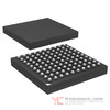
The STM32F103 family is designed for applications requiring a balance between processing power, peripheral integration, and power efficiency. The series includes up to 11 timers, 3 analog-to-digital converters, 2 digital-to-analog converters, and 13 communication interfaces, making it suitable for motor control, industrial automation, medical instrumentation, and consumer electronics. The availability of multiple package options—including LQFP64, LQFP100, LQFP144, LFBGA64, LFBGA100, and LFBGA144—allows designers to select the form factor that best matches their physical and thermal constraints.
Core Architecture and Processing Capabilities of the STM32F103
The STM32F103 employs a 32-bit ARM Cortex-M3 processor core operating as a single-core system. This architecture provides single-cycle multiplication and hardware division capabilities, enabling efficient execution of arithmetic-intensive algorithms without requiring multiple clock cycles for these operations. The processor achieves 1.25 DMIPS per megahertz at zero wait states when accessing embedded Flash memory, establishing a performance baseline for real-time applications.
The Cortex-M3 core in the STM32F103 integrates an embedded Trace Macrocell for advanced debugging and performance analysis. This feature allows developers to capture instruction execution traces and monitor system behavior without halting processor execution, facilitating non-intrusive debugging of complex firmware. The core supports both Serial Wire Debug (SWD) and JTAG interfaces, providing flexibility in debug probe selection and integration with various development environments.
Memory Organization in the STM32F103: Flash, SRAM, and External Memory Support
The STM32F103 family offers three distinct memory configurations. The STM32F103xC variant provides 256 kilobytes of Flash memory, the STM32F103xD variant includes 384 kilobytes, and the STM32F103xE variant supplies 512 kilobytes. All variants include 64 kilobytes of embedded SRAM for runtime data storage and stack operations. This memory hierarchy allows developers to select the appropriate variant based on firmware size requirements and runtime data needs.
Flash memory in the STM32F103 supports in-system programming, enabling firmware updates without removing the device from the application circuit. The Flash memory endurance specification indicates a minimum of 10,000 erase cycles, with data retention guaranteed for 20 years at 55 degrees Celsius. This specification ensures long-term reliability for applications requiring firmware updates or field reprogramming.
The STM32F103 incorporates a Flexible Static Memory Controller (FSMC) that extends the addressable memory space beyond the embedded resources. The FSMC supports connection to external SRAM, PSRAM, NOR Flash, NAND Flash, and Compact Flash devices through a parallel interface. This capability enables applications requiring large data storage or high-speed external memory access. The FSMC supports both asynchronous and synchronous memory access modes, with configurable timing parameters to accommodate various memory device characteristics.
The STM32F103 also includes an LCD parallel interface supporting both 8080 and 6800 timing modes, allowing direct connection to LCD controllers without requiring intermediate interface circuits. This integration reduces component count and simplifies PCB layout for display-based applications.
Clock Management and Power Supply Architecture in the STM32F103
The STM32F103 incorporates multiple clock sources to support diverse application requirements. The device includes an internal 8 MHz factory-trimmed RC oscillator and an internal 40 kHz RC oscillator with calibration capability. For applications requiring higher accuracy, the STM32F103 supports external crystal oscillators ranging from 4 to 16 MHz for the high-speed external (HSE) clock and a 32.768 kHz oscillator for real-time clock (RTC) applications.
A Phase-Locked Loop (PLL) multiplier allows the STM32F103 to generate the 72 MHz system clock from lower-frequency input sources. This architecture provides flexibility in clock source selection while maintaining the high-frequency operation necessary for performance-intensive tasks. The clock tree includes multiple dividers and multiplexers, enabling independent clock frequency selection for different functional blocks within the device.
The STM32F103 power supply architecture supports a nominal voltage range of 2.0 to 3.6 volts, accommodating both 3.3-volt and lower-voltage applications. The device integrates a voltage regulator that generates internal supply voltages from the external supply, reducing the number of external power supply components required. The power supply supervisor includes Power-On Reset (POR), Power-Down Reset (PDR), and a programmable Voltage Detector (PVD) that monitors the supply voltage and generates reset signals when the voltage falls below programmed thresholds.
The STM32F103 includes a VBAT supply pin that maintains power to the RTC and backup registers during system shutdown, enabling timekeeping and data retention when the main power supply is removed. This feature supports applications requiring continuous real-time clock operation or preservation of configuration data across power cycles.
Low-Power Operating Modes and Power Management in the STM32F103
The STM32F103 provides three distinct low-power operating modes to reduce power consumption in battery-powered or energy-constrained applications. The Sleep mode reduces power consumption by halting the processor clock while maintaining peripheral operation and memory contents. In Sleep mode, the device can be awakened by interrupt events, allowing responsive operation with reduced average power consumption.
The Stop mode further reduces power consumption by disabling the internal voltage regulator and halting all clock sources except the 40 kHz internal RC oscillator and external 32.768 kHz oscillator. This mode preserves SRAM and register contents while consuming significantly less power than Sleep mode. The Stop mode includes a configurable regulator setting that allows selection between run mode and low-power mode operation, providing additional power reduction options.
The Standby mode represents the lowest power consumption state, disabling all clocks and the voltage regulator while preserving only the RTC and backup registers powered by the VBAT supply. Standby mode can be exited through external reset, NRST pin assertion, or RTC alarm events. This mode is suitable for applications requiring extended periods of minimal power consumption with periodic wake-up events.
The STM32F103 includes a SysTick timer—a 24-bit downcounter—that facilitates implementation of time-based scheduling and power mode transitions. This timer operates independently of the main system clock, enabling precise timing control even during low-power mode operation.
Timer and Watchdog Functions in the STM32F103
The STM32F103 integrates up to 11 timers providing diverse timing and control functions. The device includes up to four 16-bit general-purpose timers, each capable of operating as input capture, output compare, PWM generator, or pulse counter. These timers support quadrature encoder input for motor control applications, enabling direct connection to incremental encoders without external signal conditioning.
Two 16-bit motor control PWM timers provide specialized functionality for three-phase motor control applications. These timers include dead-time generation and emergency stop capabilities, allowing safe operation of power electronic circuits. The dead-time generation prevents simultaneous conduction of complementary power switches, protecting against shoot-through faults that could damage power devices.
The STM32F103 includes two watchdog timers: an independent watchdog and a window watchdog. The independent watchdog operates from the internal 40 kHz RC oscillator, providing watchdog functionality even when the main system clock is disabled. The window watchdog allows software to define a time window during which the watchdog must be serviced, detecting both system hangs and runaway code execution.
Two 16-bit basic timers provide timing functions for driving the digital-to-analog converter (DAC), enabling generation of periodic analog waveforms. The SysTick timer, as previously mentioned, provides a 24-bit downcounter for system timing and scheduling functions.
Communication Interfaces in the STM32F103: I2C, UART, SPI, and Specialized Protocols
The STM32F103 provides comprehensive communication interface support through multiple protocols. The device includes up to two I2C interfaces supporting both standard I2C and SMBus/PMBus protocols. The I2C interfaces operate at frequencies up to the standard 400 kHz fast mode, with configurable timing parameters to accommodate various I2C device requirements.
The STM32F103 integrates up to five UART/USART interfaces supporting asynchronous serial communication. These interfaces include support for ISO 7816 smart card protocols, LIN (Local Interconnect Network) bus protocols, and IrDA (Infrared Data Association) protocols. The USART interfaces include modem control signals, enabling integration with cellular modems and other modem-based communication devices.
The device includes up to three Serial Peripheral Interface (SPI) modules, each capable of operating at data rates up to 18 megabits per second. Two of the SPI modules include I2S (Inter-IC Sound) interface capability, enabling direct connection to audio codecs and digital audio processors. The I2S interface supports Philips protocol timing, facilitating integration with standard audio components.
The STM32F103 incorporates an SDIO (Secure Digital Input/Output) interface supporting connection to SD/MMC memory cards. This interface enables integration of removable storage media for data logging, multimedia applications, or firmware updates. The SDIO interface supports both default mode and high-speed mode operation, accommodating various SD card performance levels.
CAN and USB Connectivity in the STM32F103
The STM32F103 integrates a CAN (Controller Area Network) interface implementing the CAN 2.0B Active specification. The CAN interface supports both standard 11-bit and extended 29-bit identifiers, enabling integration into automotive and industrial control networks. The CAN interface includes message filtering capabilities, allowing the microcontroller to selectively process messages based on identifier patterns.
The STM32F103 includes a USB 2.0 full-speed interface supporting data rates up to 12 megabits per second. The USB interface enables connection to host computers for firmware programming, data transfer, or human interface device (HID) applications. The USB interface includes integrated transceiver functionality, reducing the number of external components required for USB connectivity.
Analog Signal Processing: ADC and DAC in the STM32F103
The STM32F103 incorporates three 12-bit analog-to-digital converters (ADCs) providing up to 21 analog input channels. The ADCs support a conversion range from 0 to 3.6 volts, matching the device supply voltage range. Each ADC includes triple-sample-and-hold capability, enabling simultaneous sampling of multiple analog signals. The ADCs achieve 1-microsecond conversion time, supporting real-time analog signal acquisition for control and monitoring applications.
The ADC architecture includes a 12-channel direct memory access (DMA) controller that transfers conversion results directly to memory without processor intervention. This capability enables continuous analog signal acquisition with minimal processor overhead, suitable for applications requiring high-frequency data sampling or multiple simultaneous analog channels.
The STM32F103 includes two 12-bit digital-to-analog converters (DACs) providing analog output capability. The DACs support buffered and non-buffered output modes, with the buffered mode providing lower output impedance for driving external loads. The DACs can be driven by the basic timers, enabling generation of periodic analog waveforms such as sine waves or triangular waves for signal generation or audio applications.
The STM32F103 integrates an on-chip temperature sensor providing analog output proportional to die temperature. This sensor enables thermal monitoring and temperature-based system control, supporting applications requiring thermal management or temperature compensation.
Input/Output Architecture and GPIO Capabilities of the STM32F103
The STM32F103 provides up to 112 general-purpose input/output (GPIO) pins, with the specific count depending on the selected package variant. The LQFP64 package provides 51 I/O pins, the LQFP100 package provides 80 I/O pins, and the LQFP144 package provides 112 I/O pins. All GPIO pins are mappable to 16 external interrupt vectors, enabling flexible interrupt source assignment.
The GPIO architecture includes 5-volt tolerant pins on most I/O ports, allowing direct connection to 5-volt logic circuits without requiring level translation circuits. This feature simplifies integration with legacy 5-volt systems and reduces component count in mixed-voltage applications. The GPIO pins support both CMOS and TTL input characteristics, accommodating various signal source impedances and voltage levels.
The STM32F103 includes a Nested Vectored Interrupt Controller (NVIC) that manages interrupt prioritization and routing. The NVIC supports up to 16 external interrupt vectors, with configurable priority levels enabling flexible interrupt handling strategies. The External Interrupt/Event Controller (EXTI) allows configuration of interrupt triggers on rising edges, falling edges, or both, supporting diverse sensor and signal conditioning requirements.
Debug and Trace Capabilities in the STM32F103
The STM32F103 provides comprehensive debug support through the Serial Wire JTAG Debug Port (SWJ-DP), supporting both Serial Wire Debug (SWD) and JTAG interfaces. The SWD interface requires only two pins (clock and data), reducing PCB routing complexity compared to JTAG. The JTAG interface provides compatibility with legacy debug tools and supports boundary scan testing.
The embedded Trace Macrocell in the STM32F103 captures instruction execution traces, enabling non-intrusive analysis of program execution flow and performance characteristics. This capability supports debugging of complex firmware without halting processor execution, facilitating analysis of real-time system behavior.
The STM32F103 includes a 96-bit unique identifier that can be used for device identification, secure boot implementation, or firmware licensing schemes. This identifier is programmed during manufacturing and cannot be modified, providing a reliable device identification mechanism.
Package Options and Thermal Characteristics of the STM32F103
The STM32F103 is available in six package options accommodating different application requirements. The LQFP64 package (10 × 10 mm) provides a compact form factor for space-constrained applications. The LQFP100 package (14 × 14 mm) offers increased pin count while maintaining a through-hole compatible footprint. The LQFP144 package (20 × 20 mm) provides maximum pin count for applications requiring all available I/O and peripheral connections.
The LFBGA100 package (10 × 10 mm) and LFBGA144 package (10 × 10 mm) provide ball grid array options with 0.8 mm pitch, enabling high-density PCB layouts. The WLCSP64 package (4.466 × 4.395 mm) represents the most compact option, utilizing wafer-level chip-scale packaging technology for space-constrained applications.
The STM32F103 operates across a temperature range of 40 to 85 degrees Celsius, supporting industrial and commercial applications. Thermal characteristics vary by package type, with larger packages providing better heat dissipation. The device includes thermal shutdown protection that disables the voltage regulator if die temperature exceeds safe operating limits, preventing thermal damage.
Electrical Specifications and Operating Conditions for the STM32F103
The STM32F103 operates from a supply voltage range of 2.0 to 3.6 volts, accommodating both 3.3-volt and lower-voltage applications. The device includes integrated power supply decoupling and filtering, reducing the number of external capacitors required. The power supply supervisor monitors supply voltage and generates reset signals when voltage falls below programmed thresholds, ensuring reliable operation across the specified voltage range.
The STM32F103 current consumption varies significantly based on operating mode and clock frequency. In Run mode with code and data processing running from Flash memory at 72 MHz and 3.6 volts, typical current consumption is approximately 36 milliamps with peripherals enabled. Sleep mode reduces current consumption to approximately 10 milliamps, while Stop mode reduces consumption to approximately 2 milliamps. Standby mode achieves the lowest consumption at approximately 2 microamps, suitable for battery-powered applications requiring extended operational life.
The device supports external clock sources ranging from 4 to 16 MHz for the high-speed external oscillator and 32.768 kHz for the real-time clock oscillator. The internal 8 MHz RC oscillator provides factory trimming to within 1 percent accuracy, supporting applications that do not require external crystal oscillators. The internal 40 kHz RC oscillator provides calibration capability, enabling adjustment of oscillator frequency to compensate for temperature and supply voltage variations.
The STM32F103 includes a CRC (Cyclic Redundancy Check) calculation unit supporting hardware-accelerated CRC computation for data integrity verification. This feature reduces processor overhead for checksum calculations in communication protocols and data storage applications.
The device supports RoHS3 compliance and includes moisture sensitivity level 3 (168 hours), indicating compatibility with standard PCB assembly processes. The STM32F103 is not subject to REACH restrictions, simplifying regulatory compliance for applications in regulated markets.
Conclusion
The STM32F103 represents a comprehensive microcontroller solution for applications requiring substantial processing capability, extensive peripheral integration, and flexible communication options. The combination of 72 MHz ARM Cortex-M3 processing, up to 512 kilobytes of Flash memory, multiple timer functions, and 13 communication interfaces positions the STM32F103 as a versatile platform for industrial control, motor control, medical instrumentation, and consumer electronics applications. The availability of multiple package options and memory configurations enables designers to optimize cost and form factor for specific application requirements. The integrated power management features, including multiple low-power modes and programmable voltage detection, support battery-powered and energy-constrained applications. The comprehensive debug and trace capabilities facilitate firmware development and system optimization. Selection of the appropriate STM32F103 variant and package option requires careful consideration of memory requirements, I/O pin count, thermal constraints, and communication interface needs specific to each application.
Frequently Asked Questions (FAQ)
- Q1. What is the maximum operating frequency of the STM32F103, and how does this affect application performance?
-
- A1. The STM32F103 operates at a maximum frequency of 72 MHz, delivering 1.25 DMIPS per megahertz at zero wait states when accessing embedded Flash memory. This performance level supports real-time control applications, signal processing, and data acquisition tasks. The actual performance achieved depends on the specific algorithm implementation and memory access patterns. Applications with tight timing constraints should verify that the 72 MHz frequency provides sufficient computational headroom for the intended workload, accounting for interrupt latency and peripheral access overhead.
- Q2. How do the three memory variants (STM32F103xC, STM32F103xD, and STM32F103xE) differ, and how should I select the appropriate variant?
-
- A2. The STM32F103xC provides 256 kilobytes of Flash memory, the STM32F103xD provides 384 kilobytes, and the STM32F103xE provides 512 kilobytes. All variants include 64 kilobytes of embedded SRAM. Selection should be based on firmware size requirements, accounting for both code and constant data storage. Applications with large lookup tables, audio samples, or extensive string resources may require the larger memory variants. The STM32F103xE variant provides maximum flexibility for complex applications, while the STM32F103xC variant offers cost optimization for simpler applications with smaller firmware footprints.
- Q3. What are the differences between the Sleep, Stop, and Standby low-power modes, and when should each be used?
-
- A3. Sleep mode halts the processor clock while maintaining peripheral operation and memory contents, reducing power consumption to approximately 10 milliamps at 3.6 volts. This mode is suitable for applications that require rapid response to interrupt events while reducing average power consumption. Stop mode disables the internal voltage regulator and halts all clock sources except the 40 kHz internal RC oscillator and external 32.768 kHz oscillator, reducing consumption to approximately 2 milliamps. This mode is appropriate for applications that can tolerate longer wake-up latency in exchange for lower power consumption. Standby mode achieves the lowest consumption at approximately 2 microamps by disabling all clocks and the voltage regulator, preserving only the RTC and backup registers. This mode is suitable for battery-powered applications requiring extended operational life with periodic wake-up events triggered by external signals or RTC alarms.
- Q4. How many communication interfaces does the STM32F103 provide, and which interfaces are most suitable for different application types?
-
- A4. The STM32F103 provides up to 13 communication interfaces including two I2C interfaces, five UART/USART interfaces, three SPI interfaces (two with I2S capability), one SDIO interface, one CAN interface, and one USB interface. I2C interfaces are suitable for connecting sensors, memory devices, and other peripherals on a shared bus. UART/USART interfaces support serial communication with host computers, GPS receivers, and other serial devices. SPI interfaces provide high-speed communication with memory devices, analog-to-digital converters, and other SPI-compatible peripherals. I2S interfaces enable direct connection to audio codecs and digital audio processors. The CAN interface supports automotive and industrial control networks. The USB interface enables connection to host computers for programming and data transfer. The SDIO interface supports connection to SD/MMC memory cards for data logging and removable storage applications.
- Q5. What is the purpose of the Flexible Static Memory Controller (FSMC), and what types of external memory can it support?
-
- A5. The FSMC extends the addressable memory space of the STM32F103 by providing a parallel interface to external memory devices. The FSMC supports connection to external SRAM, PSRAM, NOR Flash, NAND Flash, and Compact Flash devices. This capability enables applications requiring large data storage beyond the embedded 512 kilobytes of Flash memory, such as data logging systems, multimedia applications, or systems requiring large lookup tables. The FSMC supports both asynchronous and synchronous memory access modes with configurable timing parameters, accommodating various memory device characteristics and performance requirements.
- Q6. How does the STM32F103 support motor control applications, and what specialized features are provided?
-
- A6. The STM32F103 includes two 16-bit motor control PWM timers with dead-time generation and emergency stop capabilities, enabling safe operation of three-phase motor control circuits. The general-purpose timers support quadrature encoder input for direct connection to incremental encoders, enabling closed-loop motor control without external signal conditioning. The three 12-bit ADCs with up to 21 analog input channels support current sensing and voltage monitoring for motor control feedback. The DMA controller enables continuous analog signal acquisition without processor intervention, supporting high-frequency control loops. The CAN interface enables communication with other motor control nodes in networked systems.
- Q7. What package options are available for the STM32F103, and how should I select the appropriate package for my application?
-
- A7. The STM32F103 is available in six package options: LQFP64 (10 × 10 mm, 51 I/O pins), LQFP100 (14 × 14 mm, 80 I/O pins), LQFP144 (20 × 20 mm, 112 I/O pins), LFBGA100 (10 × 10 mm, 100 I/O pins), LFBGA144 (10 × 10 mm, 144 I/O pins), and WLCSP64 (4.466 × 4.395 mm, 64 I/O pins). Selection should consider the number of I/O pins required, PCB space constraints, thermal dissipation requirements, and manufacturing capabilities. The LQFP packages provide through-hole compatible footprints suitable for prototyping and low-volume production. The BGA packages enable higher-density PCB layouts for space-constrained applications. The WLCSP64 package provides the most compact option for applications with minimal I/O requirements and severe space constraints.
- Q8. How does the STM32F103 handle analog signal acquisition, and what are the specifications of the analog-to-digital converters?
-
- A8. The STM32F103 incorporates three 12-bit ADCs providing up to 21 analog input channels with a conversion range from 0 to 3.6 volts. Each ADC achieves 1-microsecond conversion time and includes triple-sample-and-hold capability for simultaneous sampling of multiple analog signals. The ADCs support a 12-channel DMA controller that transfers conversion results directly to memory without processor intervention, enabling continuous analog signal acquisition with minimal processor overhead. Applications requiring high-frequency data sampling or multiple simultaneous analog channels should utilize the DMA capability to minimize processor load. The ADC accuracy specifications should be verified for applications requiring high-precision analog measurements, accounting for reference voltage stability and temperature variations.
- Q9. What debug and trace capabilities does the STM32F103 provide, and how do these support firmware development?
-
- A9. The STM32F103 provides Serial Wire Debug (SWD) and JTAG interfaces through the Serial Wire JTAG Debug Port (SWJ-DP). The SWD interface requires only two pins (clock and data), reducing