Product overview of STM32F103VBT7
STM32F103VBT7 is a 32-bit microcontroller from STMicroelectronics’ STM32F103xB medium-density performance line, based on the ARM Cortex-M3 core. It integrates 128 Kbytes of embedded Flash memory and 20 Kbytes of SRAM, operates up to 72 MHz, and is offered in a 100‑pin LQFP package (14 × 14 mm).
The STM32F103VBT7 combines a 32-bit CPU, a rich set of timers, advanced communication interfaces (including USB 2.0 full-speed and CAN 2.0B Active), multiple 12-bit ADC channels, a temperature sensor, and extensive GPIO capability (up to 80 I/Os). Its supply voltage range from 2.0 V to 3.6 V, extended operating temperature range from −40 °C to +105 °C (TA), and built‑in low‑power modes suit a wide variety of embedded applications, from industrial control and motor drive to communication gateways and instrumentation.
2.
Core architecture and performance of STM32F103VBT7
STM32F103VBT7 leverages an ARM 32‑bit Cortex‑M3 CPU running at a maximum frequency of 72 MHz. The core delivers 1.25 DMIPS/MHz (Dhrystone 2.1) at 0‑wait‑state memory access, providing a good balance between performance and power consumption. Single‑cycle multiplication and hardware division allow efficient implementation of numerically intensive control algorithms, digital filtering, and protocol stacks.
A nested vectored interrupt controller (NVIC) is tightly integrated with the Cortex‑M3 core in STM32F103VBT7. NVIC supports fast interrupt handling with programmable priority levels and vectored responses, improving real‑time behavior. This is valuable in applications that must respond deterministically to events such as motor commutation, communication frame reception, or time‑critical sensor sampling.
The STM32F103VBT7 also offers a serial wire and JTAG debug port (SWJ‑DP), enabling flexible debug and trace via either standard JTAG or the more pin‑efficient SWD. This unified debug access, combined with the Cortex‑M3 architecture, supports advanced development and testing workflows, such as breakpoint-based debugging, register inspection, and on‑chip flash programming.
3.
Memory subsystem of STM32F103VBT7
The memory architecture of STM32F103VBT7 is designed to support both code density and runtime performance.
– Flash memory: STM32F103VBT7 integrates 128 Kbytes of embedded Flash. This memory stores program code and, if needed, non‑volatile configuration data. Flash is organized to provide 0‑wait‑state access at lower frequencies, with internal mechanisms to sustain performance at higher clock speeds up to 72 MHz. Flash endurance and data retention characteristics are specified to support typical embedded lifecycles.
– SRAM: The device includes 20 Kbytes of SRAM. This volatile memory is used for stack, heap, and runtime data. Running time‑critical routines from SRAM can further improve execution speed and can reduce current consumption compared with Flash execution under some conditions.
– Memory mapping: STM32F103VBT7 shares the STM32F103xB memory map, which defines address regions for Flash, SRAM, peripherals, and system configuration. This deterministic address space simplifies linker configuration and supports features such as bootloader mapping and relocation of vector tables.
– CRC calculation unit: STM32F103VBT7 includes a hardware CRC unit. This block can compute CRC values on memory buffers, which is useful for verifying Flash contents on startup, checking data integrity in communication protocols, or validating configuration data structures. Offloading CRC computation from the CPU frees processing resources and shortens integrity checks.
4.
Clock, reset and power management in STM32F103VBT7
The STM32F103VBT7 clock system provides flexible clock source selection and distribution through an internal clock tree.
– Clock sources:
• High-speed external (HSE) oscillator input supports 4–16 MHz crystals or external clock sources.
• Low-speed external (LSE) oscillator supports a 32.768 kHz crystal, typically used for real‑time clock (RTC) functions.
• Internal 8 MHz RC oscillator (HSI), factory trimmed, enables operation without external crystals, simplifying designs where clock accuracy requirements are moderate.
• Internal 40 kHz RC oscillator (LSI) can be used for independent watchdog and low‑power timing functions.
– PLL: A phase-locked loop allows STM32F103VBT7 to multiply clock sources (typically the HSE or HSI) up to the 72 MHz CPU frequency. PLL configuration allows trade‑offs among performance, power consumption, and clock accuracy.
– Reset and power supervision: STM32F103VBT7 includes power‑on reset (POR), power‑down reset (PDR), and a programmable voltage detector (PVD). These blocks monitor supply levels, ensuring that code execution occurs only when the supply is within valid operating ranges. The PVD can generate interrupts or reset when the voltage passes programmable thresholds, providing protection against brown-out conditions and supply dips.
– Voltage regulator: An internal regulator in STM32F103VBT7 supplies the core domain from the external VDD pins. Its modes interact with low‑power states (Run, Sleep, Stop, Standby), enabling different power/performance profiles depending on application needs.
Real‑world example: In a mains‑powered industrial controller using STM32F103VBT7, the HSE with a precise crystal can be used for accurate timing of communication interfaces and control loops, while the PVD can monitor the DC bus. If the supply drops near the lower tolerance, the system can save critical data and initiate a controlled shutdown or restart.
5.
Low‑power modes and backup functions of STM32F103VBT7
STM32F103VBT7 supports several low‑power modes to reduce current consumption when full performance is not required:
– Sleep mode: The CPU clock is stopped while peripherals and memory remain clocked. Execution resumes quickly on an interrupt, allowing short idle periods to be exploited for power savings when peripherals (e.g., UART, timers) remain active.
– Stop mode: The main regulator can operate either in Run or Low‑power mode while the clocks are stopped. SRAM and register contents are preserved, and wakeup can be triggered via external interrupts, RTC, or other wake sources. Stop mode current is significantly lower than in Sleep mode, suitable for longer idle periods.
– Standby mode: This is the lowest‑power state in STM32F103VBT7. The internal regulator is switched off, the main SRAM content is lost, and only the backup domain and a few wakeup sources remain powered. Wakeup results in a reset‑like restart. Standby mode is suited to battery‑powered designs that remain off for extended periods but must preserve RTC time and a small amount of backup data.
– VBAT supply: STM32F103VBT7 provides a VBAT pin to supply the RTC and backup registers when the main VDD is off. This allows the RTC time and backup configuration to be maintained from a coin cell or separate backup supply, even when the primary system power is disconnected.
Using these modes, a design based on STM32F103VBT7 can scale between high‑performance operation and deep sleep, depending on system events. For instance, a data logger might run at 72 MHz only when sampling and storing data, enter Stop mode between acquisitions, and occasionally enter Standby when no events are expected for long intervals, while VBAT keeps the RTC running.
6.
Timer and watchdog resources in STM32F103VBT7
STM32F103VBT7 integrates a versatile set of timer and watchdog peripherals that support precise timing, waveform generation, and system supervision.
– General-purpose 16‑bit timers: There are three 16‑bit timers, each with up to four channels that can be configured for input capture (IC), output compare (OC), PWM generation, or pulse counting. Certain timers also support quadrature encoder interfaces for incremental position sensing. This allows direct interfacing with rotary encoders in motor or motion control applications.
– Motor control timer: A dedicated 16‑bit motor control PWM timer with dead-time generation and emergency stop input is available in STM32F103VBT7. This timer can generate complementary PWM outputs with precise dead time insertion, supporting three‑phase motor drives and similar power conversion topologies. The emergency stop input can immediately disable outputs in response to fault conditions such as over‑current.
– Watchdog timers: STM32F103VBT7 includes two watchdogs:
• Independent watchdog: Driven by its own clock source, it remains active even if the main clock fails. It is used to recover from software malfunctions by generating a reset if not periodically reloaded.
• Window watchdog: This watchdog can be configured to trigger a reset if the refresh occurs too early or too late within a defined time window, detecting both stuck and runaway software conditions.
– SysTick timer: A 24‑bit downcounter built into the Cortex‑M3 core in STM32F103VBT7 provides a standard time base, often used for operating system ticks or periodic events.
With these resources, STM32F103VBT7 can manage complex timing tasks such as multi‑channel PWM for motors, measurement of input signal frequencies, precise delays, and robust supervisory functions to enhance system robustness.
7.
Communication interfaces and connectivity options of STM32F103VBT7
Connectivity is a central feature of STM32F103VBT7, which offers up to nine communication interfaces:
– I²C interfaces: Up to 2 × I²C interfaces are supported, with SMBus/PMBus compatibility. This allows communication with a wide range of sensors, power management devices, and expansion peripherals. Each I²C can operate as master or slave and supports standard timing requirements detailed in the device characteristics.
– USARTs: STM32F103VBT7 integrates up to 3 USARTs. These support:
• Asynchronous UART mode for serial communication,
• Synchronous modes,
• LIN support,
• IrDA capability,
• ISO 7816 smart card interface,
• Modem control signals.
This breadth enables STM32F103VBT7 to connect to legacy serial devices, smart cards, infrared interfaces, and automotive or industrial serial buses using LIN.
– SPI interfaces: Up to 2 SPIs are available, supporting speeds up to 18 Mbit/s. They can operate in master or slave mode and are suitable for high‑speed sensor interfaces, external ADCs/DACs, memory devices, and inter‑MCU communication.
– CAN interface: STM32F103VBT7 includes a CAN 2.0B Active interface. It supports standard and extended frames, enabling integration in automotive, industrial, and building automation networks that rely on CAN for robust communication.
– USB interface: A USB 2.0 full-speed device interface is integrated in STM32F103VBT7. It allows direct connection to hosts for firmware update, data transfer, or human‑machine interface functions. The datasheet specifies startup time and electrical characteristics for ensuring compliance with USB full‑speed signaling.
Real‑world example: A gateway module can use STM32F103VBT7’s CAN interface to connect to a vehicle CAN bus, USB to connect to a PC service tool, and USART/I²C to interface with local sensors or expansion modules, all simultaneously while the CPU handles protocol translation.
8.
GPIO and interrupt handling in STM32F103VBT7
STM32F103VBT7 offers a large number of digital I/Os and a flexible external interrupt system.
– GPIO resources: Up to 80 fast I/O ports are available, with 26/37/51/80 I/Os depending on the package and configuration across the STM32F103xB family. In STM32F103VBT7’s 100‑pin LQFP package, many pins are available as GPIOs. Most GPIOs are 5 V‑tolerant, allowing direct interfacing with TTL‑level logic while the MCU operates at 2.0–3.6 V.
Each GPIO in STM32F103VBT7 can be configured as input, push‑pull or open‑drain output, alternate function, or analog input. Output drive characteristics and input thresholds are specified in the electrical characteristics to support correct matching with external circuitry.
– External interrupts and events: The external interrupt/event controller (EXTI) in STM32F103VBT7 can map almost all GPIOs to up to 16 external interrupt lines. These lines can be configured to trigger on rising, falling, or both edges. EXTI can also generate events to wake the device from low‑power modes without necessarily handling a full interrupt.
This combination gives STM32F103VBT7 considerable flexibility for event-driven designs. For example, an external sensor or user button can be connected to a GPIO configured as an EXTI source to wake the MCU from Stop mode, execute a short task, and return to low power, minimizing average energy consumption.
9.
Analog subsystems and temperature sensing in STM32F103VBT7
STM32F103VBT7 embeds analog functionality that supports measurement and monitoring tasks.
– A/D converters: The device includes two 12‑bit ADCs with up to 16 multiplexed channels. The converters can achieve a conversion time of 1 µs, which supports high‑speed sampling in control and measurement applications. The conversion range is 0 to 3.6 V, aligned with the analog supply rails.
Dual sample-and-hold capability allows STM32F103VBT7 to capture multiple channels nearly simultaneously, which is valuable in applications such as motor control, where phase currents must be measured at the same instant, or in multi‑channel data acquisition.
ADC accuracy, reference voltage, input impedance, and sampling characteristics are defined in the datasheet, including guidance on external resistor and capacitor selection (RAIN and sampling capacitance) and recommended connection diagrams.
– Temperature sensor: An internal temperature sensor is connected to one of the ADC channels. In STM32F103VBT7, this sensor can be used to monitor device temperature and implement thermal management policies, such as derating performance at high temperatures or logging system thermal conditions.
Typical applications: In a motor control system, STM32F103VBT7’s ADCs can measure phase currents and DC bus voltage, while the internal temperature sensor monitors device temperature. In a portable measurement instrument, multiple analog sensors can be multiplexed to the ADC inputs, with calibration carried out in software using the reference and accuracy data.
10.
DMA and data handling capabilities of STM32F103VBT7
STM32F103VBT7 integrates a 7‑channel DMA controller. The DMA can transfer data between memory and peripherals or between memory locations without CPU intervention, reducing latency and CPU load in data‑intensive applications.
Peripherals supported by DMA in STM32F103VBT7 include timers, ADCs, SPIs, I²Cs, and USARTs. For example:
– ADC + DMA: Continuous or triggered ADC conversions can be streamed into memory via DMA, enabling high‑throughput data acquisition without constant CPU servicing of end‑of‑conversion events.
– SPI/I²C/UART + DMA: Communication buffers can be filled or emptied via DMA, supporting high‑speed transfers and freeing the core to process data instead of handling every byte.
– Timer + DMA: Timers can interact with DMA to update PWM duty cycles or capture values automatically, enabling advanced waveform generation or signal capture schemes.
Real‑world example: In a motor drive using STM32F103VBT7, ADCs capture phase currents synchronized with PWM timers. DMA transfers the conversion results into a memory buffer, while the CPU focuses exclusively on control loop computations at a fixed rate, improving both efficiency and control quality.
11.
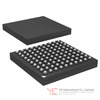
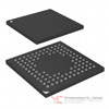
Package, pinout and mechanical characteristics of STM32F103VBT7
STM32F103VBT7 is supplied in a 100‑pin low-profile quad flat package (LQFP100) with a 14 × 14 mm body size. The package offers:
– 0.5 mm pin pitch, suitable for standard PCB fabrication processes.
– Sufficient pin count for exposing up to 80 GPIOs along with all the communication interfaces, timers, analog inputs, and power pins.
Mechanical and thermal characteristics of the LQFP100 package are documented, including:
– Dimensions and recommended PCB footprint to ensure correct soldering and mechanical reliability.
– Thermal parameters (e.g., maximum power dissipation Pp vs ambient temperature TA) that help in thermal budgeting. These parameters allow estimation of junction temperature under expected load conditions, guiding heatsinking, PCB copper area, and enclosure design.
Since STM32F103VBT7 belongs to a family with multiple package options (VFQFPN36, LQFP48, LQFP64, LQFP100, TFBGA64, LFBGA100), the 100‑pin LQFP variant offers the highest I/O and peripheral availability, which is beneficial when multiple interfaces and analog inputs must coexist in the same design.
12.
Electrical characteristics and operating conditions of STM32F103VBT7
STM32F103VBT7 complies with defined electrical and environmental conditions that frame its use in real products.
– Supply voltage: The application supply and I/Os operate from 2.0 V to 3.6 V. Electrical parameters such as logic thresholds, output drive, and ADC ranges are specified within this range.
– Operating temperature: STM32F103VBT7 is specified for −40 °C to +105 °C ambient (TA). This extended range enables use in demanding environments such as automotive compartments, industrial cabinets, or outdoor systems.
– Current consumption: The datasheet provides typical and maximum currents for:
• Run mode at different frequencies, with code executing from Flash or RAM, and with peripherals enabled or disabled.
• Sleep mode currents with different configurations.
• Stop and Standby mode currents, with data showing their variation versus temperature and supply voltage.
These data points allow precise power budgeting and battery-life estimation.
– Clock source characteristics: Electrical characteristics for the high-speed external oscillator (HSE) and low-speed external oscillator (LSE) include required load capacitances, drive levels, and startup times. For internal oscillators (HSI, LSI), accuracy and temperature dependence are provided.
– I/O characteristics: STM32F103VBT7’s I/O static and dynamic characteristics include input leakage, output voltage levels at specified currents, rise/fall times, and ESD robustness. Timing constraints are given for communication interfaces (I²C, SPI, USB, USART), ensuring that external components and traces can be dimensioned to meet protocol requirements.
– Memory characteristics: Flash access time, endurance, and data retention are specified. This helps determine firmware update strategies, logging schemes, and long‑term reliability of program storage in STM32F103VBT7-based systems.
– EMC and electrical sensitivity: The device’s EMC behavior and ESD/EMI ratings are documented, including EMS/EMI characteristics and absolute maximum ratings for electrostatic discharge and other stresses. These figures support PCB layout and protection component selection.
13.
Compliance, reliability and family compatibility of STM32F103VBT7
STM32F103VBT7 adheres to environmental and export regulations and aligns with a wider family of STM32F103 devices.
– Environmental compliance: STM32F103VBT7 is RoHS3 compliant and has a moisture sensitivity level (MSL) of 3 (168 hours). This classification informs storage and handling procedures during manufacturing, including baking and floor life limits. The device is also listed as REACH unaffected.
– Export classification: STM32F103VBT7 is classified under ECCN 3A991A2 and HTSUS 8542.31.0001, which can be relevant for global logistics and trade compliance processes.
– Family compatibility: STM32F103VBT7 belongs to the STM32F103xB medium‑density performance line, which also includes devices such as STM32F103RB, STM32F103CB, and related x8/xB family members. Full compatibility is maintained throughout the family in terms of core architecture and main peripheral sets, allowing pin‑for‑pin or software‑level migration between memory sizes and packages in many cases.
This compatibility supports platform designs where a PCB may be populated with STM32F103VBT7 for feature‑rich variants or with smaller-members such as STM32F103RB/CB/V8 etc. for cost‑optimized versions, while reusing firmware and hardware as much as possible.
14.
Conclusion on STM32F103VBT7
STM32F103VBT7 integrates a 72 MHz ARM Cortex‑M3 core, 128 Kbytes of Flash, 20 Kbytes of SRAM, versatile timers, two 12‑bit ADCs, a temperature sensor, and a comprehensive connectivity set including CAN and USB full-speed, all in a 100‑pin LQFP package. Its 2.0–3.6 V operating range, extended temperature capability, low‑power modes, and robust clock and power supervision make it suitable for a broad spectrum of embedded control, communication, and measurement applications.
The combination of hardware CRC, 7‑channel DMA, NVIC, flexible GPIO and EXTI, along with environmental compliance and family compatibility, enables STM32F103VBT7 to serve as a core building block in both new designs and existing STM32F103 platforms requiring the feature set and pin count of the 100‑pin LQFP variant.
Frequently Asked Questions (FAQ)
- Q1. What core and maximum clock frequency does STM32F103VBT7 use?
-
- A1. STM32F103VBT7 uses an ARM 32‑bit Cortex‑M3 core running at up to 72 MHz. The core delivers 1.25 DMIPS/MHz (Dhrystone 2.1) with 0‑wait‑state memory access under appropriate conditions.
- Q2. How much Flash and RAM are integrated in STM32F103VBT7?
-
- A2. STM32F103VBT7 integrates 128 Kbytes of embedded Flash memory for code and non‑volatile data and 20 Kbytes of SRAM for runtime data. Flash organization and access times are specified in the device’s memory characteristics, supporting code execution at the full 72 MHz operating frequency.
- Q3. What package does STM32F103VBT7 come in, and how many GPIOs are available?
-
- A3. STM32F103VBT7 is offered in a 100‑pin LQFP package with a 14 × 14 mm body. In this configuration, it provides up to 80 fast I/O ports, many of which are 5 V‑tolerant and mappable to external interrupt lines.
- Q4. What is the operating voltage and temperature range of STM32F103VBT7?
-
- A4. The application supply (VDD) and I/Os of STM32F103VBT7 operate from 2.0 V to 3.6 V. The device supports an ambient operating temperature range from −40 °C to +105 °C (TA), with thermal characteristics specifying the allowed power dissipation as a function of temperature.
- Q5. Which communication interfaces are integrated in STM32F103VBT7?
-
- A5. STM32F103VBT7 provides up to nine communication interfaces, including up to 2 × I²C (SMBus/PMBus), up to 3 × USARTs (with LIN, IrDA, ISO 7816, and modem control), up to 2 × SPIs (up to 18 Mbit/s), a CAN 2.0B Active interface, and a USB 2.0 full-speed device interface.
- Q6. Does STM32F103VBT7 support USB, and what type?
-
- A6. Yes. STM32F103VBT7 integrates a USB 2.0 full-speed interface that operates as a device, allowing direct connection to USB hosts. The datasheet provides startup time, DC electrical characteristics, and full‑speed electrical parameters for correct interface design.
- Q7. What analog capabilities does STM32F103VBT7 provide?
-
- A7. STM32F103VBT7 includes two 12‑bit ADCs with up to 16 channels, a conversion time of 1 µs, and a conversion range of 0–3.6 V. It also integrates an internal temperature sensor connected to the ADC, enabling on‑chip temperature monitoring. The datasheet details ADC accuracy, sampling characteristics, and recommended connection diagrams.
- Q8. What timers are available in STM32F103VBT7 for motor control and timing tasks?
-
- A8. STM32F103VBT7 offers three 16‑bit general-purpose timers, each with up to four IC/OC/PWM channels and optional quadrature encoder inputs. It also includes a dedicated 16‑bit motor control PWM timer with dead‑time insertion and emergency stop input. Additionally, there are two watchdog timers (independent and window) and a 24‑bit SysTick timer.
- Q9. How does STM32F103VBT7 handle low‑power operation?
-
- A9. STM32F103VBT7 supports Sleep, Stop, and Standby modes. Sleep mode halts the CPU clock while keeping peripherals active. Stop mode stops the clocks but retains SRAM and register contents, with wakeup via interrupts or RTC. Standby mode turns off the internal regulator and loses main SRAM content, preserving only the backup domain and enabling wakeup via dedicated sources. A VBAT supply input powers the RTC and backup registers when VDD is off.
- Q10. Does STM32F103VBT7 include DMA, and which peripherals are supported?
-
- A10. Yes. STM32F103VBT7 features a 7‑channel DMA controller that supports transfers for timers, ADCs, SPIs, I²Cs, and USARTs. DMA allows data movement between peripherals and memory or memory‑to‑memory transfers without CPU involvement, improving throughput and reducing CPU overhead.
- Q11. How are interrupts and external events handled in STM32F103VBT7?
-
- A11. STM32F103VBT7 uses a nested vectored interrupt controller (NVIC) integrated with the Cortex‑M3 core for fast, prioritized interrupt handling. An external interrupt/event controller (EXTI) maps GPIO lines to up to 16 external interrupt lines, configurable for various trigger edges. EXTI can also generate events for waking the device from low‑power modes.
- Q12. Is there a hardware CRC unit in STM32F103VBT7, and what is it used for?
-
- A12. STM32F103VBT7 includes a CRC calculation unit that can compute CRC values over memory buffers in hardware. This is used for verifying Flash contents at startup, ensuring data integrity in stored data or communication protocols, and reducing the CPU load associated with software CRC calculation.
- Q13. What environmental and export classifications apply to STM32F103VBT7?
-
- A13. STM32F103VBT7 is RoHS3 compliant and has a moisture sensitivity level (MSL) of 3 with a floor life of 168 hours. It is listed as REACH unaffected. Export classification includes ECCN 3A991A2 and HTSUS 8542.31.0001, which may be used in logistics and compliance documentation.
- Q14. How does STM32F103VBT7 fit within the STM32F103 family?
-
- A14. STM32F103VBT7 is part of the STM32F103xB medium‑density performance line. The family includes devices such as STM32F103C8, STM32F103R8, STM32F103V8, STM32F103T8, STM32F103RB, STM32F103VB, and STM32F103CB. These devices share core architecture and peripheral sets with differing memory sizes, packages, and I/O counts. Full compatibility throughout the family allows hardware and software reuse and migration between variants.
- Q15. What watchdog options are built into STM32F103VBT7 for system reliability?
-
- A15. STM32F103VBT7 integrates two watchdogs: an independent watchdog, clocked from its own dedicated oscillator, capable of resetting the system if not refreshed in time; and a window watchdog that resets the device if refreshed too early or too late relative to a programmable window. Both enhance robustness against software failures and unexpected lockups.
- Q16. Which clock sources can be used with STM32F103VBT7, and how are they configured?
-
- A16. STM32F103VBT7 can use an external high-speed oscillator (HSE) with 4–16 MHz crystals or external clocks, an external low-speed oscillator (LSE) at 32.768 kHz, an internal 8 MHz RC oscillator (HSI), and an internal 40 kHz RC oscillator (LSI). A PLL multiplies these sources to reach the 72 MHz system clock. The clock tree allows selection and prescaling of the system, AHB, and APB clocks to match performance and power requirements.
- Q17. What should be considered for PCB layout and thermal design with STM32F103VBT7?
-
- A17. For STM32F103VBT7 in the LQFP100 package, PCB layout should follow the recommended footprint and pad dimensions given in the mechanical section. Adequate decoupling capacitors should be placed near power pins, with separate analog and digital decoupling in line with the datasheet’s reference schematics. Thermal characteristics, such as maximum power dissipation versus ambient temperature, guide the use of copper planes and airflow to keep junction temperatures within specified limits.
- Q18. Does STM32F103VBT7 support a real‑time clock and backup domain?
-
- A18. Yes. STM32F103VBT7 includes an RTC that can be clocked from a 32.768 kHz LSE crystal. A dedicated backup domain, powered via VBAT when main VDD is off, preserves the RTC and backup registers across power cycles or Standby mode, enabling timekeeping and retention of small configuration sets even when the main system is off.