Hello Guest

Sign in / Register

Welcome,{$name}!

/ Logout
English
EnglishDeutschItaliaFrançais한국의русскийSvenskaNederlandespañolPortuguêspolski繁体中文SuomiGaeilgeSlovenskáSlovenijaČeštinaMelayuMagyarországHrvatskaDanskromânescIndonesiaΕλλάδαБългарски езикGalegolietuviųMaoriRepublika e ShqipërisëالعربيةአማርኛAzərbaycanEesti VabariikEuskeraБеларусьLëtzebuergeschAyitiAfrikaansBosnaíslenskaCambodiaမြန်မာМонголулсМакедонскиmalaɡasʲພາສາລາວKurdîსაქართველოIsiXhosaفارسیisiZuluPilipinoසිංහලTürk diliTiếng ViệtहिंदीТоҷикӣاردوภาษาไทยO'zbekKongeriketবাংলা ভাষারChicheŵaSamoaSesothoCрпскиKiswahiliУкраїнаनेपालीעִבְרִיתپښتوКыргыз тилиҚазақшаCatalàCorsaLatviešuHausaગુજરાતીಕನ್ನಡkannaḍaमराठी
STM32F103VDT7 Image

View larger Image

Image may be representation.
See specs for product details.

STM32F103VDT7

Manufacturer Part Number: STM32F103VDT7
Manufacturer/Brand: STMicroelectronics
Part of Description: IC MCU 32BIT 384KB FLASH 100LQFP
Datasheets: 1.STM32F103VDT7.pdf 2.STM32F103VDT7.pdf 3.STM32F103VDT7.pdf
RoHs Status: Lead free / RoHS Compliant
Stock Condition: 4744 pcs Stock
Ship From: Hong Kong
Shipment Way: DHL/Fedex/TNT/UPS/EMS

Request Quote

Please complete all required fields with your contact information.Click "SUBMIT REQUEST" we will contact you shortly by email. Or Email us: Info@Y-IC.com.

Part No.
Quantity
Target Price(USD)

Inquiry Online

  • Contact Name
  • Company
  • E-mail
  • Phone
  • Message
  • Verify
  • Specifications
  • QC & Packaging
  • Shipping
  • Payment
  • Part NumberSTM32F103VDT7
  • ManufacturerSTMicroelectronics
  • DescriptionIC MCU 32BIT 384KB FLASH 100LQFP
  • CategoryIntegrated Circuits (ICs) > Embedded - Microcontrollers
  • Part Status4744 pcs Stock
  • Voltage - Supply (Vcc/Vdd)2V ~ 3.6V
  • Supplier Device Package100-LQFP (14x14)
  • Speed72MHz
  • SeriesSTM32F1
  • RAM Size64K x 8
  • Program Memory TypeFLASH
  • Program Memory Size384KB (384K x 8)
  • PeripheralsDMA, Motor Control PWM, PDR, POR, PVD, PWM, Temp Sensor, WDT
  • Package / Case100-LQFP
  • PackageTray
  • Oscillator TypeInternal
  • Operating Temperature-40°C ~ 105°C (TA)
  • Number of I/O80
  • Mounting TypeSurface Mount
  • EEPROM Size-
  • Data ConvertersA/D 16x12b; D/A 2x12b
  • Core Size32-Bit Single-Core
  • Core ProcessorARM® Cortex®-M3
  • ConnectivityCANbus, I²C, IrDA, LINbus, SPI, UART/USART, USB
  • Base Product NumberSTM32F103
  • STM32F103VDT7 Details PDFSTM32F103VDT7 PDF - DE.pdf

QC (Quality Warranty)

All products are carefully inspected before shipment according to our Quality Management practices. We ensure each part is genuine, meets specification requirements, and is functionally checked against original datasheets.
Our quality process supports reliable part performance and minimized risk of defects in customer applications.

Visual Inspection X-Ray Analysis Decapsulation Analysis Spectrometer Dimension Verification Dimension Verification Dimension Verification

Packaging

ESD Protection & Handling

All ESD-sensitive components are handled under anti-static control procedures.
Products are sealed in ESD-safe packaging to prevent electrostatic damage.
Proper labeling is applied for identification and traceability.
This ensures product integrity during storage, handling, and shipment.

Global Shipment by DHL/FedEx/TNT/UPS

Delivery time
Deliverytime will need 2-4days to most of country all over the world for DHL/UPS/FEDEX/TNT.
Shipping fees reference DHL.
1). You can offer your express delivery account for shipment, ifyou haven’t any express account for shipment, we can offer our account inadvance.
2). Use our account for shipment, Shipment charges(ReferenceDHL, Different Countries has different price.)

Shipment charges: (Reference DHL)
Weight(KG) Price(USD$)
0.00kg-1.00kg USD$60.00
1.00kg-2.00kg USD$70.00
2.00kg-3.00kg USD$80.00

More details: https://www.yic-electronics.com/shipment-way.htm
Please feel free contact us. Send any inquires or question toour Email Info@YIC-Electronics.com
We can do the best to you. Thank you very much your support.

Payment Way: Wire Transfer = Telegraphic Transfer(T/T) or PayPal or Western Union

Wire Transfer (T/T)

Our HSBC bank name: The Hongkong and Shanghai Banking Corporation Limited (HSBC Hong Kong)

Benefit Company Name: YIC International Co., Limited
Bank charges and payment account details, please click "Payment Way".

Western Union


Complete payment by Western Union.
Step 1. Go to your local Western Union branch, or go to their website (www.westernunion.com)
Step 2. Follow their instructions.


Bank charges and payment account details, please click "Payment Way".

PayPal Account:

PayPal Golden Key Supplier

PayPal Account:
PayPal Account ID: Info@YIC-Electronics.com
Company: YIC International Co., Limited

If you want to pay via Credit Card, please choose "Pay with my PayPal account" to continue by paypal.(www.paypal.com
Bank charges details, please click "Payment Way".

STM32F103VDT7 from STMicroelectronics: A Detailed Look at the STM32F103xD Performance-Line Microcontroller

STM32F103VDT7 product overview

The STM32F103VDT7 is a 32-bit microcontroller from STMicroelectronics based on the Arm Cortex-M3 core. It belongs to the STM32F1 performance line and, more specifically, to the STM32F103xD group. The device combines a maximum CPU frequency of 72 MHz with embedded Flash memory, SRAM, a broad set of digital communication interfaces, analog peripherals, multiple timers, and support for low-power operating modes.

In the configuration referenced for STM32F103VDT7, the device provides 384 Kbytes of Flash memory, 64 Kbytes of SRAM, and up to 80 I/O pins in a 100-pin LQFP package measuring 14 × 14 mm. It operates from a 2.0 V to 3.6 V supply range and supports an ambient temperature range up to 105°C for the listed variant. The product integrates USB 2.0 full-speed, CAN 2.0B active, SDIO, up to five USARTs, up to three SPIs with I2S capability on two of them, and up to two I2C interfaces.

The broader STM32F103xC, STM32F103xD, and STM32F103xE datasheet describes this series as offering up to 11 timers, 3 ADCs, and 13 communication interfaces, with package options ranging from WLCSP64 to LQFP144 and BGA formats. Within that series context, STM32F103VDT7 represents a high-density member that balances memory size, interface breadth, and package accessibility.

STM32F103VDT7 position within the STM32F103xC, STM32F103xD, and STM32F103xE family

The STM32F103VDT7 is part of a family structured around three memory-density groups: STM32F103xC, STM32F103xD, and STM32F103xE. Across these groups, STMicroelectronics maintains broad architectural and peripheral compatibility, allowing design migration based on memory, package, and I/O requirements rather than requiring a full platform redesign.

In this family:

STM32F103xC devices are positioned in the 256 Kbyte Flash class.

STM32F103xD devices, including STM32F103VDT7, occupy the intermediate 384 Kbyte Flash class.

STM32F103xE devices extend to 512 Kbytes of Flash.

This arrangement helps when a design begins in one memory tier and later grows. If firmware expands because of a larger protocol stack, additional buffering, or more application logic, migration within the same family can preserve much of the hardware and software structure. The datasheet also indicates package options with 64, 100, and 144 pins, plus BGA and WLCSP versions, which supports scaling in both board area and I/O count.

The “VD” portion of STM32F103VDT7 identifies the 100-pin package and the 384 Kbyte Flash class. For designs requiring more external connections than 64-pin versions can offer, while avoiding the board area of 144-pin packages, this package point can fit between compact and maximum-I/O implementations.

STM32F103VDT7 processing architecture and memory organization

At the core of the STM32F103VDT7 is the Arm 32-bit Cortex-M3 CPU, operating at up to 72 MHz. STMicroelectronics specifies a performance level of 1.25 DMIPS/MHz using Dhrystone 2.1, with 0 wait-state memory access under stated conditions. The core also includes single-cycle multiplication and hardware division, which supports faster execution in control loops, protocol handling, and arithmetic-heavy firmware routines.

The memory subsystem includes:

384 Kbytes of embedded Flash

64 Kbytes of embedded SRAM

The embedded Flash stores application code and nonvolatile data. The SRAM serves runtime variables, stacks, communication buffers, and temporary processing space. The datasheet also describes a CRC calculation unit, which can be used for data integrity checks, firmware verification, or communication frame validation.

The STM32F103xD architecture also supports a flexible static memory controller, or FSMC, with four chip-select signals. This enables interfacing with external SRAM, PSRAM, NOR Flash, NAND memory, and CompactFlash. For applications that outgrow internal memory or need direct parallel-memory connection, the FSMC broadens system design options without requiring a separate external bus controller.

The family memory map is defined in the datasheet, which helps developers place code, data, peripheral registers, and external memory resources correctly. In practical terms, this structure matters when firmware needs to split tasks between fast internal execution and larger external data storage. For example, an application can keep real-time control logic in internal Flash and SRAM while using FSMC-connected memory for data logging or a user-interface frame buffer.

STM32F103VDT7 clock system, startup behavior, and boot modes

The STM32F103VDT7 supports multiple clock sources to accommodate different precision, startup, and power-consumption targets. According to the datasheet, the available clock elements include:

A 4 MHz to 16 MHz external crystal oscillator

An internal 8 MHz factory-trimmed RC oscillator

An internal 40 kHz RC oscillator with calibration

A 32 kHz oscillator for the RTC with calibration

A PLL for clock multiplication

This combination allows the system to be built around an external crystal for tighter timing accuracy, or around internal RC oscillators when reducing component count is preferred. The clock tree described in the datasheet distributes these sources to the CPU core and peripherals, making it possible to tailor peripheral clocks independently from the primary execution clock.

Startup behavior and reset sequencing are tied to the integrated clock, reset, and supply-management blocks. The STM32F103VDT7 also supports multiple boot modes. These boot modes define where execution begins after reset, which can be used for normal application startup or for loading firmware through supported programming paths.

In a practical development scenario, boot-mode flexibility is useful during manufacturing and field updates. A board may boot from the main Flash during normal operation, while development or service procedures can use an alternate boot path for programming or recovery.

STM32F103VDT7 power supply structure, reset supervision, and low-power operation

The STM32F103VDT7 operates from a 2.0 V to 3.6 V application supply for both the core and I/Os. The datasheet describes several integrated supply-management and supervisory functions:

POR (power-on reset)

PDR (power-down reset)

Programmable voltage detector (PVD)

Integrated voltage regulator

VBAT supply for RTC and backup registers

These functions help maintain controlled startup and operation as the supply rises, falls, or experiences threshold conditions. The VBAT domain allows the real-time clock and backup registers to remain powered even when the main supply is absent.

The STM32F103VDT7 also supports three low-power modes:

Sleep

Stop

Standby

These modes provide different tradeoffs between state retention, wake-up time, and current consumption. Sleep mode keeps more of the device active for shorter wake-up latency. Stop mode reduces current further while retaining more context than Standby. Standby mode minimizes power draw more aggressively and is suited to systems that spend long periods inactive.

The datasheet includes current-consumption tables for Run, Sleep, Stop, and Standby modes, as well as temperature and voltage dependency curves. It also provides wake-up timing data. This allows designers to estimate battery life and compare mode selection against system responsiveness.

For instance, a data logger that samples periodically might run acquisition and communication tasks at 72 MHz, then enter Stop mode between measurements. A mains-powered industrial node, by contrast, may remain in Run mode continuously and use lower-power states only during communication idle periods.

STM32F103VDT7 timer resources, watchdogs, and real-time support

The STM32F103VDT7 belongs to a family that provides up to 11 timers. These include:

Up to four 16-bit general-purpose timers, each with up to 4 IC/OC/PWM channels or pulse counter and quadrature encoder input

2 × 16-bit motor-control PWM timers with dead-time generation and emergency stop

2 × watchdog timers: Independent Watchdog and Window Watchdog

SysTick 24-bit downcounter

2 × 16-bit basic timers to drive the DAC

This timer set supports a broad range of timing and control functions. General-purpose timers can generate PWM, measure pulse width, count external events, or decode incremental encoder inputs. Motor-control timers add hardware features for power-stage driving, including dead-time insertion and emergency stop behavior. Basic timers are intended to trigger DAC activity, while SysTick can support periodic operating-system ticks or scheduler timing.

The Independent Watchdog and Window Watchdog provide two supervisory approaches. The former is suited to recovering from software lockups when the application fails to refresh the watchdog. The latter can also detect timing faults where software refreshes too early or too late.

The family also includes an RTC with backup registers. This lets the STM32F103VDT7 maintain timekeeping and preserve selected state information from the VBAT supply domain when the main application power is removed.

STM32F103VDT7 communication interfaces and data-transfer capabilities

One of the defining characteristics of the STM32F103VDT7 is the range of integrated communication blocks. The datasheet describes up to 13 communication interfaces across the family, and for this device class the available functions include:

Up to 2 × I2C interfaces with SMBus/PMBus support

Up to 5 USARTs with support for ISO 7816, LIN, IrDA, and modem control

Up to 3 SPI interfaces, with 2 supporting I2S multiplexing

CAN 2.0B active

USB 2.0 full speed

SDIO

This set allows a single controller to bridge several serial standards at once. For example, one USART can be assigned to a maintenance console, another to a field bus bridge, I2C to sensors or power-management devices, SPI to high-speed converters or display controllers, CAN to automotive or industrial networking, and USB to a host-connected service interface.

The datasheet also specifies DMA support through a 12-channel DMA controller. Supported DMA targets include timers, ADCs, DAC, SDIO, I2S, SPI, I2C, and USARTs. DMA reduces CPU involvement in repetitive transfers, which can improve throughput and reduce interrupt load.

A practical example is an application that samples analog channels, moves conversion results into memory by DMA, packets the data for USB or CAN transmission, and simultaneously maintains a UART diagnostic link. Without DMA, the CPU would spend more time moving data between peripherals and memory. With DMA, more execution time remains available for processing and control algorithms.

STM32F103VDT7 analog functions, sensing features, and signal-conversion resources

The STM32F103VDT7 family integrates substantial analog capability. According to the datasheet, the series includes:

3 × 12-bit ADCs with 1 μs conversion time

Up to 21 ADC channels

Triple sample-and-hold capability

2 × 12-bit DACs

Integrated temperature sensor

The ADC conversion range is 0 V to 3.6 V. This supports direct sampling of a wide set of conditioned analog signals, provided the signal stays within the permitted range and reference arrangement. The datasheet also includes ADC electrical characteristics, accuracy tables, maximum input impedance guidance, and example connection diagrams, along with decoupling recommendations for VDDA and VREF+ arrangements.

The DAC channels allow generation of analog output waveforms or reference levels. Since the family also provides basic timers to drive the DAC, waveform generation can be handled with coordinated timing.

The integrated temperature sensor offers an internal measurement point for monitoring device temperature behavior. While it is not a substitute for every external sensing task, it can support thermal supervision, compensation, or diagnostics within the system.

In application terms, the STM32F103VDT7 can combine signal acquisition, local processing, and analog output in one device. A control node, for example, may read multiple analog inputs through the ADCs, compute a response, and output an analog control voltage through the DAC while also reporting status over CAN or USB.

STM32F103VDT7 GPIO structure, interrupt handling, and debug support

The STM32F103VDT7 is listed with up to 80 I/Os in the 100-pin package variant. In the broader family, devices can provide 51, 80, or 112 I/Os depending on package. The datasheet states that almost all I/Os are 5 V-tolerant, and all can be mapped onto 16 external interrupt vectors.

This makes the GPIO subsystem suitable for dense mixed-signal and mixed-interface designs. The external interrupt/event controller (EXTI) allows GPIO pins to trigger interrupts or events, while the NVIC manages interrupt prioritization and handling at the core level. Together, these blocks support responsive firmware behavior for communication events, user inputs, protection circuits, or timing-related external signals.

The STM32F103VDT7 also provides serial wire debug (SWD) and JTAG interfaces through the serial wire/JTAG debug port, with support for the Cortex-M3 Embedded Trace Macrocell. This gives access to standard debugging functions and trace capability for firmware bring-up and runtime analysis.

For firmware development, this combination is practical because it allows low-pin-count SWD debugging in production-style board layouts, while retaining more extensive JTAG and trace options when supported by the hardware design.

STM32F103VDT7 external memory expansion and display interface options

Beyond its internal memory resources, the STM32F103VDT7 family includes the FSMC, which supports external static memories and certain parallel devices. The controller offers four chip-select signals and supports:

CompactFlash

SRAM

PSRAM

NOR memory

NAND memory

The datasheet also notes LCD parallel interface support in 8080 and 6800 modes. This makes the STM32F103VDT7 suitable for systems that need a parallel display connection or external memory-mapped display controller.

These capabilities are useful in designs where embedded graphics, data storage, or high-bandwidth parallel access are needed. For example, an HMI panel may use the FSMC to connect a parallel LCD while also using external SRAM or NOR memory for assets and buffers. The timing tables and waveform diagrams provided in the datasheet help determine whether a given external memory or display interface can be matched to the STM32F103VDT7 bus timing.

STM32F103VDT7 package, pin-count, and operating-condition considerations

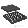
The STM32F103VDT7 is available in a 100-pin LQFP package with 14 × 14 mm body dimensions. Within the family, package options also include LQFP64, LQFP144, LFBGA100, LFBGA144, and WLCSP64. This range allows the same core architecture and broad peripheral structure to be used across boards with different mechanical and routing constraints.

For the STM32F103VDT7 specifically, the 100-LQFP package provides a middle-ground option. It offers more I/O access than 64-pin variants while remaining easier to inspect and assemble than finer-pitch BGA or WLCSP options in many manufacturing environments.

The datasheet includes package mechanical drawings, recommended PCB footprint information, and thermal characteristics. These are relevant not only for layout, but also for soldering profile planning, enclosure integration, and thermal analysis.

Operating conditions covered in the datasheet include:

General operating conditions

Power-up and power-down conditions

Reset and power-control block characteristics

Clock-source characteristics

PLL characteristics

I/O characteristics

Temperature sensor characteristics

Communication-interface electrical specifications

This breadth means package and operating-condition selection should be treated together. For instance, package choice affects available I/Os and thermal behavior, while oscillator choice influences timing accuracy and startup characteristics.

STM32F103VDT7 electrical characteristics and practical selection considerations

The STM32F103VDT7 datasheet provides detailed electrical data across supply current, timing, analog performance, interface specifications, and environmental sensitivity. A few selection parameters stand out directly from the provided documentation:

Maximum core frequency: 72 MHz

Supply voltage range: 2.0 V to 3.6 V

Program memory: 384 Kbytes Flash

RAM: 64 Kbytes SRAM

I/O count: up to 80

ADC resolution: 12-bit

DAC resolution: 12-bit

USB: full-speed

CAN: 2.0B active

Package: 100-LQFP

Moisture sensitivity level: MSL 3

RoHS status: RoHS3 compliant

REACH status: REACH unaffected

The current-consumption tables are useful when comparing the STM32F103VDT7 against devices with similar CPU speed but different peripheral density. The communication-interface timing tables help verify compatibility with external devices before schematic completion. The ADC and DAC specifications clarify expected analog performance under stated conditions rather than relying only on nominal resolution numbers.

A practical device-selection flow for the STM32F103VDT7 often comes down to several questions:

Does the application fit within 384 Kbytes Flash and 64 Kbytes SRAM?

Are 80 I/Os sufficient in the selected package?

Is 72 MHz enough for the control and communication load?

Are USB, CAN, SDIO, multiple serial ports, and timer resources all needed on one device?

Is the 2.0 V to 3.6 V operating range aligned with the board power architecture?

Is the 100-LQFP package the preferred balance of I/O access, footprint, and assembly method?

If the answer to these questions remains aligned with the project requirements, the STM32F103VDT7 sits in a part of the STM32F103 family that offers relatively high integration without moving to the largest package tier.

Conclusion

The STM32F103VDT7 from STMicroelectronics is a high-density STM32F1 performance-line microcontroller built around a 72 MHz Arm Cortex-M3 core with 384 Kbytes of Flash and 64 Kbytes of SRAM. In addition to its processing capability, the device combines extensive communication support, broad timer resources, integrated ADC and DAC functions, low-power operating modes, and external-memory expansion through the FSMC.

Its place within the STM32F103xD group gives it a clear role between lower-density and higher-density family members, while family-wide compatibility supports design scaling across memory and package options. The 100-pin LQFP format, up to 80 I/Os, USB, CAN, SDIO, multiple serial interfaces, and mixed-signal resources make the STM32F103VDT7 suitable for designs that need a single controller to coordinate control, communication, conversion, and interface tasks.

Frequently Asked Questions (FAQ)

Q1. What core does the STM32F103VDT7 use?
A1. The STM32F103VDT7 uses an Arm Cortex-M3 32-bit single-core CPU.
Q2. What is the maximum operating frequency of the STM32F103VDT7?
A2. The STM32F103VDT7 operates at up to 72 MHz.
Q3. How much Flash memory is available in the STM32F103VDT7?
A3. The STM32F103VDT7 provides 384 Kbytes of embedded Flash memory.
Q4. How much SRAM does the STM32F103VDT7 include?
A4. The STM32F103VDT7 includes up to 64 Kbytes of SRAM.
Q5. Which STM32F103 family group does the STM32F103VDT7 belong to?
A5. The STM32F103VDT7 belongs to the STM32F103xD group within the STM32F103xC, STM32F103xD, and STM32F103xE family.
Q6. What package is used by the STM32F103VDT7?
A6. The STM32F103VDT7 is specified in a 100-pin LQFP package with 14 × 14 mm dimensions.
Q7. How many I/O pins are available on the STM32F103VDT7?
A7. The STM32F103VDT7 provides up to 80 I/Os in the 100-pin package variant.
Q8. What supply voltage range does the STM32F103VDT7 support?
A8. The STM32F103VDT7 supports a 2.0 V to 3.6 V application supply and I/O range.
Q9. Does the STM32F103VDT7 support USB?
A9. Yes. The STM32F103VDT7 includes a USB 2.0 full-speed interface.
Q10. Does the STM32F103VDT7 include a CAN interface?
A10. Yes. The STM32F103VDT7 supports CAN 2.0B active.
Q11. What serial communication interfaces are available on the STM32F103VDT7?
A11. The STM32F103VDT7 supports up to 2 I2C interfaces, up to 5 USARTs, up to 3 SPIs, I2S on 2 of the SPI interfaces, USB, CAN, and SDIO.
Q12. Does the STM32F103VDT7 support DMA?
A12. Yes. The STM32F103VDT7 family includes a 12-channel DMA controller supporting peripherals such as timers, ADCs, DAC, SDIO, I2S, SPI, I2C, and USARTs.
Q13. How many ADCs are available in the STM32F103VDT7 family?
A13. The STM32F103VDT7 family includes 3 × 12-bit ADCs with conversion time down to 1 μs and up to 21 channels.
Q14. Does the STM32F103VDT7 have DAC outputs?
A14. Yes. The STM32F103VDT7 family includes 2 × 12-bit DACs.
Q15. Is there an internal temperature sensor in the STM32F103VDT7?
A15. Yes. The STM32F103VDT7 includes an integrated temperature sensor.
Q16. What timer resources are available on the STM32F103VDT7?
A16. The STM32F103VDT7 family provides up to 11 timers, including general-purpose 16-bit timers, motor-control PWM timers, basic timers, watchdog timers, and the SysTick timer.
Q17. Does the STM32F103VDT7 support motor-control functions?
A17. Yes. The STM32F103VDT7 family includes 2 × 16-bit motor-control PWM timers with dead-time generation and emergency stop.
Q18. What watchdog options does the STM32F103VDT7 provide?
A18. The STM32F103VDT7 includes two watchdogs: an Independent Watchdog and a Window Watchdog.
Q19. Does the STM32F103VDT7 include RTC capability?
A19. Yes. The STM32F103VDT7 includes an RTC and backup registers, with VBAT support for retaining operation when the main supply is removed.
Q20. What low-power modes are supported by the STM32F103VDT7?
A20. The STM32F103VDT7 supports Sleep, Stop, and Standby modes.
Q21. Which clock sources can be used with the STM32F103VDT7?
A21. The STM32F103VDT7 supports a 4 MHz to 16 MHz external crystal oscillator, an internal 8 MHz factory-trimmed RC oscillator, an internal 40 kHz RC oscillator with calibration, a 32 kHz RTC oscillator with calibration, and a PLL.
Q22. Does the STM32F103VDT7 support boot configuration options?
A22. Yes. The STM32F103VDT7 supports multiple boot modes for defining startup behavior after reset.
Q23. Can the STM32F103VDT7 interface with external memory?
A23. Yes. The STM32F103VDT7 family includes an FSMC with four chip-select signals supporting CompactFlash, SRAM, PSRAM, NOR, and NAND memories.
Q24. Can the STM32F103VDT7 drive parallel LCD interfaces?
A24. Yes. The STM32F103VDT7 family supports an LCD parallel interface in 8080 and 6800 modes.
Q25. Are the GPIOs on the STM32F103VDT7 5 V tolerant?
A25. The datasheet states that almost all GPIOs are 5 V tolerant.
Q26. How are external interrupts handled in the STM32F103VDT7?
A26. All I/Os can be mapped onto 16 external interrupt vectors through the EXTI system, with interrupt handling managed by the NVIC.
Q27. What debug interfaces are available on the STM32F103VDT7?
A27. The STM32F103VDT7 supports SWD and JTAG through the SWJ-DP and also includes Cortex-M3 Embedded Trace Macrocell support.
Q28. How does the STM32F103VDT7 fit within the STM32F103 memory-density lineup?
A28. The STM32F103VDT7 sits between the STM32F103xC devices with 256 Kbytes of Flash and the STM32F103xE devices with 512 Kbytes of Flash, offering 384 Kbytes in the STM32F103xD class.
Q29. What practical applications benefit from the STM32F103VDT7 communication mix?
A29. Based on the integrated interfaces, the STM32F103VDT7 can be used in systems that need to combine USB, CAN, serial ports, sensor buses, and memory-card connectivity within one controller, such as control nodes, data concentrators, or embedded human-machine interfaces.
Q30. What makes the STM32F103VDT7 suitable for mixed-signal embedded designs?
A30. The STM32F103VDT7 combines 12-bit ADCs, 12-bit DACs, an internal temperature sensor, timers, DMA, and multiple communication interfaces, allowing signal acquisition, local processing, and digital connectivity within one microcontroller.
Slide the scroll wheel to view more.
Click to see more

User Review

  • Jack***III

    Good price

    May 15th, 2026

  • Davi***ung

    Good SoC for networking applications. Stable signal processing and low power consumption.

    May 6th, 2026

  • Andr***ee

    Overall is good

    April 28th, 2026

  • Emil***ark

    Accurate frequency output for timing circuits. Works well in low-power signal designs.

    April 23th, 2026

  • Jose***Dong

    Quick response and clear answers.

    April 16th, 2026

  • Marc***echLab

    Excellent quality. All chips passed testing and showed consistent electrical characteristics.

    April 7th, 2026

  • Circ***MasterX

    Good packaging and fast shipping. Performance is stable, but I wish there was clearer labeling on each component.

    April 2th, 2026

  • SamT***Reviews

    Excellent ICs. Used them in a communication module and performance was stable.

    March 27th, 2026

  • Kevi***.

    Good quality parts. No failures during testing.

    March 17th, 2026

  • Bria***.

    Good

    March 13th, 2026

  • Mari***.

    Superb performance.

    March 2th, 2026

  • Emma***

    Excellent ICs for DIY projects. Came well-packaged, genuine parts, and all tested good on my bench. No fails on 50 pieces.

    February 26th, 2026

  • Gadg***an123

    Good

    February 10th, 2026

  • Quan***PartsLab

    Great service

    February 6th, 2026

  • Vect***upplyChain

    The sales rep was professional and responsive.

    January 27th, 2026

  • Puls***vePurchasing

    Components were packed carefully with anti-static protection and cushioning. Everything arrived in good condition.

    January 23th, 2026

  • Pixe***ocure

    Components were packed well. Appreciated the attention to detail.

    January 13th, 2026

  • Byte***dgeBuyer

    Good Quality & Fast Response

    January 5th, 2026

  • Circ***AtlasGlobal

    JUST WHAT I WANT

    December 30th, 2025

  • Allo***taImports

    Very professional

    December 26th, 2025

  • Apex***i

    Quick response and prompt shipping

    December 19th, 2025

  • Hexa***e Circuits

    We were surprised by how quickly our order was processed. From inquiry to delivery, everything was smooth. A trustworthy IC distributor with good stock levels.

    December 11th, 2025

  • Core***se Inc.

    Good customer service

    December 2th, 2025

  • Skyl***Drew

    Delivered ahead of schedule.

    November 28th, 2025

  • Byte***ad

    We purchased a batch of XC6SLX25T-2CSG324C from yic-electronics. Clean markings, fresh 2024 date codes, and antistatic packaging—service was efficient and polite.

    November 17th, 2025

  • avl_***rcing_julia

    Smooth checkout and same-day ship via FedEx. Parts arrived dry-packed, correct MSL labels, and fresh date codes.

    November 13th, 2025

  • Liam***hnson

    Price is good. Order processed quickly, and tracking provided the same night.

    November 3th, 2025

  • Yuko***kamura

    Prices were reasonable compared to other brokers. One reel had minor box damage, but the inner pack was intact.

    October 31th, 2025

  • Opti***

    Excellent prices and top-notch customer service. Even the standard shipping was surprisingly fast. Components were well-packed and genuine. Totally satisfied with the purchase.

    October 21th, 2025

  • Thom***Gray

    Clear communication and on-time delivery.

    October 15th, 2025

  • Aaro***ughes

    Excellent supplier. Great communication and reliable service throughout the process.

    October 9th, 2025

  • Auro***hip

    Good experience overall. The order was processed smoothly, packaging was secure, and the delivery time was acceptable.

    September 29th, 2025

  • Jimm***

    I had a great experience with this company. They were very professional and efficient, and they had the obsolete parts I needed in stock. Once payment was processed, the delivery was quick—my goods arrived within two weeks. The customer service was friendly professional, with seamless communication throughout. Overall, everything went smoothly, and I would definitely recommend them.

    September 19th, 2025

  • Jaso***in

    The purchase was easy and fast. Polite and helpful seller, great price.

    September 8th, 2025

  • NeoB***

    Schnelle Lieferung, Produkt entspricht der Beschreibung, hochwertige Verarbeitung, stabile Funktion, alles passt perfekt, sehr zufrieden mit dem Kauf.

    September 2th, 2025

  • Tobi***

    Quick response, good price and clear communication. Very satisfied with the service

    August 28th, 2025

  • Zóc***Nights

    Not bad

    August 19th, 2025

  • 3174***41@gmail.com

    Bought once to know that YIC electronic components quality is good, and the price is not expensive, very affordable, fast delivery!
    Really recommend buying electronic components here!

    April 14th, 2025

  • Yush***nagahata

    YIC is an excellent company.
    The deliverry time is fast, and we find it very usueful for procuring electronic components.
    We look forward to continuing our relationship in the future.
    Go YIC! Keep up the great work!

    February 20th, 2025

  • SAMI*** INSTALLATION

    Fantastic! Shure I would buy again with YIC

    January 23th, 2025

  • Aadh***x

    The experience with YIC International was great. They not only provided support for the proposed parts but also proactively suggested additional parts that could be useful for us. They have reviewed all the parts properly and corrected our requirements. The delivery and other logistical support were excellent.

    January 22th, 2025

  • Ke*

    A Reliable and Trustworthy Partner
    Received original, high-quality components with fast shipping from YIC electronics.

    November 25th, 2024

  • Nana***risnawan

    Great component supplier, a place that easy to find electronics parts at a good price and delivery.

    August 6th, 2024

  • Alge***n Gholson

    Great products, fast delivery.
    The quality and service of YIC Electronics' components are at the top of the industry. Highly recommended.

    February 20th, 2024

  • Frey***.

    Our partnership with YIC Electronics has been exceptionally satisfying. Their unwavering commitment to outstanding customer service, coupled with their highly competitive pricing and unwavering dedication to top-notch, high-performance product quality, has consistently impressed us. YIC Electronics stands out as a true industry leader in every aspect of their service. Their swift and efficient logistics feedback further underscores their professionalism and reliability.

    August 25th, 2023

  • Jo C***n

    High Quality Products!
    I received genuine, high-quality electronic parts. Thank you YIC electronics.

    August 12th, 2023

  • Edwa***W.

    Yic-electronics suppliers are top notch quality and consistent reliability, I have generated several orders from their website and their service has exceeded expectations in providing electronic components for our business needs.

    August 6th, 2023

  • Anna***

    Yic-electronics is a good partner for our company, we have been cooperating with each other for 4 years, and the cooperation is all smooth and there is no dispute about the goods. Our latest transaction with Yic-electronics happened a month ago, and the process was very smooth, thanks to Yic-electronics's help!

    June 17th, 2023

0 Articles

Post a Review

Hello , welcome to comment on this product
Rating *
5.0

Please limit the remark to 500 words

Your personal information will be hidden

FAQFrequently Asked Questions

  • When considering the STM32F103VDT7 for a new design requiring significant data acquisition, what are the practical implications of its 16x12-bit ADCs, particularly concerning sample rate limitations and potential for crosstalk in high-density sensor arrays? The STM32F103VDT7 features 16 analog inputs, each with a 12-bit resolution, suitable for general-purpose analog-to-digital conversion. However, achieving the maximum theoretical sample rate for all 16 channels simultaneously will be constrained by the microcontroller's clock speed and the ADC conversion time. For high-density sensor arrays where precise timing and isolation between channels are critical, designers should carefully analyze the ADC conversion sequence and consider multiplexing strategies or external sample-and-hold circuits if channel-to-channel crosstalk becomes a concern at higher frequencies or with varying analog signal levels. The 72MHz clock speed of the STM32F103VDT7 provides a good basis, but the specific ADC clock prescaler selection will directly impact the effective sample rate per channel.
  • For applications demanding robust communication protocols like CANbus and LINbus with the STM32F103VDT7, what are the typical performance bottlenecks to anticipate, and how can software and hardware optimizations mitigate them? While the STM32F103VDT7 integrates CANbus and LINbus controllers, real-world performance, especially under heavy bus load or with multiple concurrent communication tasks, can be influenced by interrupt handling latency and the overall system bus bandwidth. Effective mitigation strategies involve prioritizing critical communication interrupts, ensuring efficient data buffering in firmware to minimize DMA contention, and carefully managing the peripheral clock distribution to dedicate sufficient bandwidth to these communication interfaces. Understanding the STM32F103VDT7’s DMA capabilities and its interaction with the AHB/APB bus structure is crucial for optimizing data throughput and avoiding transmission delays.
  • Given the 384KB of FLASH memory on the STM32F103VDT7, what are the design considerations for firmware partitioning, especially when incorporating RTOS, extensive peripheral drivers, and user application code, to avoid memory fragmentation or performance degradation? With 384KB of FLASH on the STM32F103VDT7, efficient firmware architecture is paramount. Designers should consider a modular approach for code organization, separating bootloaders, RTOS kernel, drivers, and application logic. Techniques like scatter loading during the build process can optimize memory usage. It's also important to account for potential future firmware updates, leaving adequate overhead for new features or bug fixes. The 72MHz operating speed of the STM32F103VDT7 means that code execution speed from FLASH is generally good, but complex code sections or deeply nested function calls can still impact real-time performance, so profiling is recommended.
  • When designing PCBs for the STM32F103VDT7 in its 100-LQFP (14x14mm) package, what are the critical considerations for high-speed signal routing and power delivery integrity to avoid signal integrity issues and noise coupling? The 100-LQFP (14x14mm) package of the STM32F103VDT7 requires careful PCB layout. For high-speed signals, particularly those connected to SPI, UART, or USB peripherals, maintaining controlled impedance traces, minimizing trace lengths, and ensuring adequate ground plane coverage are essential to prevent reflections and signal degradation. Power delivery integrity for the 2V to 3.6V operating range of the STM32F103VDT7 necessitates a robust power distribution network with sufficient decoupling capacitors placed as close as possible to the power pins to mitigate transient voltage drops and filter out high-frequency noise.
  • For applications operating near the upper end of the STM32F103VDT7's -40°C to 105°C (TA) temperature range, what are the implications for component derating, clock speed stability, and peripheral functionality? Operating the STM32F103VDT7 at elevated ambient temperatures, approaching 105°C, can impact performance. While the device is rated for this range, factors like self-heating due to high clock speeds (72MHz) and significant peripheral activity should be considered. Excessive temperature can lead to reduced component lifespan and potentially affect the stability of internal oscillators. Engineers should perform thermal analysis and consider heatsinking or airflow strategies if the STM32F103VDT7 is expected to operate in demanding thermal environments. Derating of external components connected to the STM32F103VDT7 might also be necessary.
  • How does the 64K x 8 RAM size on the STM32F103VDT7 influence the feasibility of running complex RTOS tasks, large data buffers, or computationally intensive algorithms, and what strategies can be employed to optimize its use? The 64K x 8 (which translates to 64KB) of RAM on the STM32F103VDT7 is a significant factor for applications utilizing an RTOS or requiring substantial data buffering. For complex real-time operating systems with many tasks, extensive inter-task communication, or large data structures, this RAM might become a limiting factor. Developers should carefully profile memory usage, prioritize critical data, and consider dynamic memory allocation strategies to avoid heap fragmentation. For computationally intensive algorithms, optimizing code for minimal stack usage and leveraging DMA for data transfers can help reduce RAM pressure on the STM32F103VDT7.
  • In scenarios where the STM32F103VDT7 is integrated into systems with multiple voltage domains, what are the potential challenges related to its 2V-3.6V supply range and its interaction with peripherals operating at different voltage levels? The 2V-3.6V supply range for the STM32F103VDT7 offers flexibility, but when interfacing with peripherals that operate at different voltage levels (e.g., 5V tolerant inputs or outputs), level shifting is often required. Designers must ensure that the voltage differences do not exceed the absolute maximum ratings of the STM32F103VDT7's I/O pins. Careful selection of level shifters or voltage translators, considering their speed and current drive capabilities, is crucial to maintain signal integrity and prevent damage to either the STM32F103VDT7 or the connected peripherals.
  • For embedded systems requiring precise timing and control, such as motor control applications utilizing the STM32F103VDT7's Motor Control PWM, what are the key considerations for minimizing PWM jitter and ensuring accurate phase synchronization? The STM32F103VDT7's dedicated Motor Control PWM capabilities are beneficial for applications like motor drivers. To minimize PWM jitter and ensure accurate phase synchronization, engineers should pay close attention to the configuration of the Timer peripherals used for PWM generation, particularly the clock source and prescaler settings. Using the highest possible timer clock frequency, carefully managing interrupt priorities if feedback mechanisms are involved, and ensuring proper signal routing on the PCB to avoid noise coupling onto PWM outputs are critical. The 72MHz core clock of the STM32F103VDT7 provides a solid foundation for generating precise PWM signals.
  • When evaluating the STM32F103VDT7 for legacy system integration or as a potential upgrade path, what are the key differences and potential compatibility issues to consider compared to earlier generations of STM32F1 series microcontrollers? The STM32F103VDT7 is part of the STM32F1 series, which offers a well-established architecture. When considering it for upgrades, the primary differences will typically lie in peripheral set enhancements, memory density (384KB FLASH, 64KB RAM in this case), and potentially clock speed improvements. For compatibility, pin-to-pin compatibility within the same package type is often maintained for basic functionality. However, applications heavily relying on specific peripheral configurations or timing-critical operations might require careful re-evaluation of register settings and interrupt handling due to subtle differences in peripheral behavior or clocking schemes that may exist between different STM32F103 variants or generations.
  • For automotive or industrial applications requiring high reliability and extended operational life, what are the specific considerations regarding the STM32F103VDT7's RoHS 3 compliance and its inherent robustness in demanding environments? RoHS 3 compliance for the STM32F103VDT7 indicates adherence to material restrictions, which is a baseline for environmental responsibility. For automotive and industrial applications demanding high reliability, engineers should look beyond RoHS compliance to STMicroelectronics' specific product qualification data, which might include AEC-Q100 (for automotive) or similar industrial certifications, though these are not explicitly stated for the STM32F103VDT7. The operating temperature range of -40°C to 105°C is a good starting point, but thorough environmental testing under application-specific conditions (vibration, humidity, EMC) is crucial to validate the STM32F103VDT7's long-term performance and reliability.
  • In power-sensitive applications utilizing the STM32F103VDT7, what are the effective strategies for minimizing power consumption, particularly when operating at its maximum 72MHz speed and utilizing peripherals like CANbus or USB? Minimizing power consumption with the STM32F103VDT7, especially at 72MHz, involves judicious use of its power-saving modes. Employing strategies such as scaling down the CPU clock speed when full performance is not required, disabling unused peripherals (e.g., turning off ADC, UART, or timers when not in use), and leveraging low-power modes like Sleep or Stop mode are essential. For communication peripherals like CANbus or USB, ensuring efficient data packet handling and minimizing active transmission times can significantly reduce power draw. The STM32F103VDT7's internal oscillator can also contribute to power savings over external crystals when high precision is not strictly necessary.
  • When selecting between the STM32F103VDT7 and other variants within the STM32F1 series, what are the critical decision factors related to FLASH and RAM size for projects with uncertain future scalability requirements? The STM32F103VDT7 offers 384KB of FLASH and 64KB of RAM, which is a substantial amount within the STM32F1 series. When considering future scalability, engineers should assess the growth trajectory of their firmware and data requirements. If there's a strong possibility of significantly larger codebases or extensive data logging, exploring STM32F1 series variants with even larger FLASH or RAM, or considering a migration to a more capable series (like STM32F4 or STM32H7), might be prudent. However, for many applications, the STM32F103VDT7 provides ample headroom for growth, especially when code optimization techniques are employed.
  • For designs involving multiple sensors connected to the STM32F103VDT7's 16 ADCs, what are the potential issues with analog signal conditioning and impedance matching to ensure accurate readings across all input channels simultaneously? Accurate readings across all 16 ADC channels of the STM32F103VDT7 depend heavily on proper analog signal conditioning. Each sensor's output impedance, along with the input impedance of the STM32F103VDT7's ADC pins, can form voltage dividers that lead to inaccurate readings, especially if sensor output impedances vary significantly. Using buffer amplifiers with low output impedance between the sensors and the microcontroller's ADC inputs is a common and effective practice to mitigate these effects. Ensuring that the signal source for each ADC channel is strong and stable is crucial for achieving the full 12-bit resolution.
  • How does the internal oscillator of the STM32F103VDT7 compare in terms of accuracy and stability to an external crystal oscillator, and in which applications would the trade-offs be most significant? The STM32F103VDT7 features an internal High-Speed Internal (HSI) clock, typically around 8MHz, which is convenient and saves board space and component cost. However, it is generally less accurate and stable than an external crystal oscillator, particularly over wide temperature variations or with voltage fluctuations. For applications where precise timing is critical, such as USB communication (which requires a specific clock frequency), real-time control loops with tight tolerances, or precise frequency generation, an external crystal is highly recommended for the STM32F103VDT7. For less demanding applications, the internal oscillator may suffice.
  • When integrating the STM32F103VDT7 into a system with existing USB peripherals, what are the considerations for achieving reliable USB connectivity, including potential issues with enumeration and data transfer rates? The STM32F103VDT7 features a full-speed USB 2.0 interface. Achieving reliable USB connectivity requires careful adherence to USB protocol specifications. This includes proper implementation of the USB stack in firmware, ensuring correct USB signal routing on the PCB with controlled impedance, and appropriate termination. Issues with enumeration can often stem from incorrect timing of USB setup packets or power supply noise. For optimal data transfer rates, designers should leverage DMA to offload the CPU and ensure the overall system clocking is stable and configured correctly for the USB peripheral.
  • For applications using the STM32F103VDT7 in high-vibration environments, what are the potential reliability concerns related to its surface mount package and internal components? While the STM32F103VDT7 is a surface-mount device (SMD) in a 100-LQFP package, and generally robust, high-vibration environments can pose challenges. The solder joints connecting the component to the PCB are the primary point of mechanical stress. Ensuring adequate PCB design, proper solder joint formation, and potentially mechanical support for the board can mitigate risks. Internal components and connections within the STM32F103VDT7 are typically well-protected by the epoxy encapsulation, but extreme or prolonged vibration could theoretically lead to micro-fractures or stress on internal connections over time.
  • What are the implications of using the STM32F103VDT7's PDR (Power-On Reset) and POR (Power-On Reset) features for system startup stability and preventing unintended resets during normal operation? The Power-On Reset (POR) and Power-Down Reset (PDR) features of the STM32F103VDT7 are crucial for ensuring stable system startup and preventing erroneous behavior. These circuits monitor the supply voltage and assert a reset when the voltage drops below a predefined threshold, ensuring that the microcontroller begins operation in a known, defined state. In applications where the power supply might fluctuate or experience brownout conditions, these features are invaluable. Proper configuration and understanding of their reset thresholds are important to avoid unintended resets during normal operation while still providing adequate protection against power disturbances.
  • When considering the STM32F103VDT7 for long-term projects, what is the typical product lifecycle and obsolescence risk associated with this series of microcontrollers from STMicroelectronics? The STM32F1 series, including the STM32F103VDT7, has been a popular and well-established product line from STMicroelectronics. While STMicroelectronics generally maintains good product availability for their core families, the lifecycle of any semiconductor component should be considered for long-term projects. Engineers should consult STMicroelectronics' official product longevity information or contact their sales representatives for specific end-of-life (EOL) forecasts or product change notification (PCN) policies related to the STM32F103VDT7. For very long-term deployments, proactive planning for potential component obsolescence or alternative sourcing strategies is advisable.