Product Overview of the STM32F103 Series
The STM32F103 represents a medium-density performance line of 32-bit microcontrollers built around the ARM Cortex-M3 architecture. This device family bridges the gap between entry-level microcontrollers and high-performance processors, offering a balanced combination of computational power, peripheral integration, and energy efficiency. The STM32F103 is manufactured by STMicroelectronics and operates at a maximum frequency of 72 MHz, delivering 1.25 DMIPS per megahertz at zero wait-state memory access.
The medium-density STM32F103 family encompasses two primary variants: the STM32F103x8 with 64 kilobytes of Flash memory and the STM32F103xB with 128 kilobytes of Flash memory. Both variants share identical peripheral configurations and pin assignments, allowing seamless migration between memory densities during product development. The device family is available in multiple package options ranging from 36 pins to 100 pins, accommodating diverse application requirements from space-constrained designs to feature-rich implementations.
The STM32F103 operates from a 2.0 to 3.6 volt power supply and is available in two temperature ranges: the industrial range from -40 to 85 degrees Celsius and the extended range from -40 to 105 degrees Celsius. This flexibility enables deployment across consumer electronics, industrial control systems, medical devices, automotive peripherals, and telecommunications equipment.
Core Architecture and Processing Capabilities of the STM32F103
The STM32F103 employs the ARM Cortex-M3 processor, a 32-bit RISC core specifically designed for embedded systems requiring high code efficiency within constrained memory environments. The processor executes the Thumb-2 instruction set, which provides a unique advantage: it delivers performance comparable to 32-bit ARM processors while maintaining code density similar to 16-bit instruction sets. This characteristic makes the STM32F103 particularly suitable for applications where memory bandwidth and storage capacity are limited.
The Cortex-M3 core within the STM32F103 incorporates several architectural features that enhance real-time performance. Single-cycle multiplication and hardware division operations eliminate the need for software-based arithmetic routines, reducing interrupt latency and improving deterministic behavior in time-critical applications. The processor supports a maximum clock frequency of 72 MHz, achieved through an internal phase-locked loop that multiplies external clock sources.
The STM32F103 achieves its 1.25 DMIPS per megahertz performance metric when executing code from Flash memory with zero wait states. This performance level is maintained across the full operating frequency range when appropriate memory access timing is configured. The processor's ability to execute instructions at this rate while maintaining low power consumption makes it suitable for applications requiring sustained computational performance without excessive thermal dissipation.
Memory Organization and Management in the STM32F103
The STM32F103 integrates three distinct memory regions: embedded Flash memory for program storage, embedded SRAM for runtime data, and a backup domain for low-power data retention. The Flash memory capacity varies between the STM32F103x8 (64 kilobytes) and STM32F103xB (128 kilobytes) variants, allowing developers to select the appropriate density for their application requirements.
The embedded SRAM capacity is fixed at 20 kilobytes across all medium-density variants. This SRAM operates at CPU clock speed with zero wait states, enabling rapid data access during program execution. The SRAM is organized as a unified memory space, allowing flexible allocation between stack, heap, and static data structures. The memory controller automatically adjusts Flash access timing based on the configured CPU frequency, inserting wait states when necessary to maintain data integrity at higher clock speeds.
The STM32F103 incorporates a cyclic redundancy check calculation unit that operates on 32-bit data words using a fixed generator polynomial. This hardware CRC engine enables runtime verification of Flash memory integrity, supporting compliance with industrial safety standards such as EN/IEC 60335-1. The CRC unit computes signatures of executing code, which can be compared against reference values generated during the build process and stored at predetermined memory locations.
The backup domain within the STM32F103 contains ten 16-bit registers capable of storing 20 bytes of user application data. These registers maintain their contents when the main power supply is removed, provided that the VBAT pin receives power from a backup battery or capacitor. This feature enables applications to preserve critical state information across power cycles, supporting use cases such as real-time clock calibration, configuration parameters, and error logging.
Power Supply and Management Features of the STM32F103
The STM32F103 requires multiple power supply connections to support its diverse functional blocks. The primary power supply, designated VDD, operates in the 2.0 to 3.6 volt range and provides power to the core processor, memory, and digital peripherals. The analog power supply, designated VDDA, operates in the same voltage range but must be isolated from the digital supply through filtering to minimize noise coupling into analog circuits. A maximum voltage difference of 300 millivolts between VDD and VDDA is tolerated during normal operation.
The VBAT pin provides an independent power supply for the real-time clock, backup registers, and the 32 kilohertz oscillator. This pin accepts voltages between 1.8 and 3.6 volts and can be powered from a backup battery when the main power supply is absent. The VBAT supply path includes an internal power switch that automatically selects between the main VDD supply and the backup supply based on voltage levels.
The STM32F103 incorporates an integrated power-on reset circuit that monitors the VDD supply and maintains the device in reset mode when the supply voltage falls below a specified threshold. This power-on reset function operates automatically without requiring external components, simplifying board design. The device also features a programmable voltage detector that monitors VDD and VDDA supplies, comparing them against selectable threshold voltages. When the supply voltage crosses a programmed threshold, the voltage detector can generate an interrupt, allowing the application to implement graceful shutdown procedures or activate backup power supplies.
The internal voltage regulator within the STM32F103 operates in three distinct modes. The main regulation mode provides nominal voltage regulation during normal operation. The low-power regulation mode reduces quiescent current during Stop mode operation. The power-down mode, used during Standby mode, disconnects the regulator output, reducing standby current to near-zero levels at the cost of losing register and SRAM contents.
Clock Generation and System Timing in the STM32F103
The STM32F103 incorporates multiple clock sources to support diverse application requirements and power management strategies. The high-speed internal RC oscillator operates at 8 megahertz with factory trimming and serves as the default clock source on device reset. This internal oscillator enables immediate operation without external components, supporting rapid prototyping and emergency fallback operation if external oscillators fail.
The high-speed external oscillator accepts crystal or ceramic resonator inputs in the 4 to 16 megahertz range. The STM32F103 monitors the external oscillator for failure and automatically switches to the internal RC oscillator if oscillation ceases, generating a software interrupt to alert the application. This clock failure detection mechanism enhances system reliability in applications where external oscillator failure could cause operational disruption.
The low-speed external oscillator operates at 32.768 kilohertz and is typically driven by a dedicated crystal resonator. This oscillator provides the clock source for the real-time clock and backup domain, enabling accurate timekeeping even when the main processor is in low-power modes. The low-speed oscillator can also serve as a calibration reference for the internal low-speed RC oscillator.
The internal low-speed RC oscillator operates at approximately 40 kilohertz and provides a clock source for the independent watchdog timer and real-time clock when external oscillators are unavailable. This oscillator operates independently of the main clock domain, allowing watchdog functionality to persist during Stop and Standby modes.
The phase-locked loop within the STM32F103 multiplies the external clock source to generate the system clock. The PLL accepts input frequencies from 4 to 16 megahertz and produces output frequencies up to 72 megahertz. The multiplication factor is programmable, allowing flexible clock generation from various external oscillator frequencies. When the high-speed internal RC oscillator is used as the PLL input, the maximum achievable system clock is limited to 64 megahertz.
The STM32F103 provides multiple prescalers that divide the system clock to generate independent clock domains. The AHB prescaler divides the system clock for the processor and memory bus, with a maximum frequency of 72 megahertz. The high-speed APB prescaler divides the AHB clock for high-speed peripherals, also with a maximum frequency of 72 megahertz. The low-speed APB prescaler divides the AHB clock for low-speed peripherals, with a maximum frequency of 36 megahertz. This hierarchical clock distribution enables independent frequency scaling of different functional blocks, optimizing power consumption for specific peripheral requirements.
Low-Power Operating Modes of the STM32F103
The STM32F103 supports three distinct low-power modes that provide different trade-offs between power consumption, wakeup latency, and available wakeup sources. These modes enable applications to minimize energy consumption during idle periods while maintaining responsiveness to external events.
Sleep mode represents the shallowest low-power state. In this mode, the processor clock is halted, but all peripheral clocks continue operating. The processor can be awakened by any interrupt or event, with wakeup latency measured in microseconds. Sleep mode is suitable for applications that require frequent processor activity but can tolerate brief periods of inactivity between processing tasks.
Stop mode achieves significantly lower power consumption by disabling all clocks in the 1.8 volt domain, including the phase-locked loop and both internal and external oscillators. The voltage regulator can operate in either normal or low-power mode during Stop mode, with low-power mode providing reduced quiescent current at the cost of longer wakeup latency. The SRAM and register contents are preserved during Stop mode, enabling rapid resumption of application execution. The device can be awakened from Stop mode by any external interrupt line, the programmable voltage detector output, the real-time clock alarm, or the USB wakeup signal.
Standby mode provides the lowest power consumption by completely disabling the internal voltage regulator and powering down the entire 1.8 volt domain. The phase-locked loop, internal oscillators, and external oscillators are all disabled. The SRAM and register contents are lost during Standby mode, except for the backup domain registers which retain their contents. The device exits Standby mode when an external reset is applied, the independent watchdog generates a reset, a rising edge appears on the wakeup pin, or the real-time clock alarm occurs.
The wakeup time from Stop or Standby mode depends on the clock source selected for resumption. When the internal RC oscillator is used, wakeup occurs within approximately 5 microseconds. When an external oscillator is required, wakeup latency increases to accommodate oscillator startup time, typically ranging from 1 to 10 milliseconds depending on the oscillator characteristics.
Interrupt and Event Handling in the STM32F103
The STM32F103 incorporates a nested vectored interrupt controller that manages up to 43 maskable interrupt channels in addition to the 16 interrupt lines provided by the Cortex-M3 core. The interrupt controller supports 16 priority levels, allowing fine-grained prioritization of interrupt sources. The closely coupled architecture of the interrupt controller minimizes interrupt latency by passing the interrupt entry vector address directly to the processor core.
The interrupt controller implements several advanced features that enhance real-time performance. Tail-chaining allows the processor to service a higher-priority interrupt that arrives while processing a lower-priority interrupt without saving and restoring the processor state. Interrupt nesting enables lower-priority interrupts to be preempted by higher-priority interrupts, ensuring that time-critical events receive immediate attention. The processor automatically saves the execution state when an interrupt occurs and restores it upon interrupt exit, eliminating instruction overhead associated with context switching.
The external interrupt and event controller provides 19 edge detector lines that can generate interrupt or event requests. Each line can be independently configured to trigger on rising edges, falling edges, or both. The controller maintains a pending register that tracks the status of interrupt requests, allowing software to determine which external events have occurred. Up to 80 general-purpose input/output pins can be connected to the 16 external interrupt lines, providing flexible event routing.
The external interrupt controller can detect pulses shorter than the internal APB2 clock period, enabling detection of brief transient events. This capability is particularly useful in applications requiring detection of short-duration signals such as button presses or sensor pulses.
Timer and Watchdog Functions of the STM32F103
The STM32F103 integrates seven timer modules that support diverse timing and counting applications. The advanced-control timer, designated TIM1, provides three-phase pulse-width modulation with complementary outputs and programmable dead-time insertion. The dead-time feature prevents shoot-through current in motor drive applications by ensuring that complementary switches do not conduct simultaneously. The advanced-control timer can generate up to six independent PWM outputs with 0 to 100 percent modulation capability.
Three general-purpose timers, designated TIM2, TIM3, and TIM4, provide 16-bit counting with up to four independent channels per timer. Each channel can be configured for input capture, output compare, PWM generation, or one-pulse mode operation. The general-purpose timers support both edge-aligned and center-aligned PWM modes, with center-aligned mode providing reduced harmonic distortion in motor control applications. The timers can be synchronized with each other through the timer link feature, enabling coordinated operation for complex timing sequences.
The STM32F103 incorporates two watchdog timers that monitor application execution and generate resets if the application fails to service the watchdog within a specified time window. The independent watchdog operates from a dedicated 40 kilohertz internal oscillator and functions independently of the main clock domain, allowing watchdog operation to persist during Stop and Standby modes. The independent watchdog can be configured through option bytes to operate in either watchdog mode or free-running timer mode.
The window watchdog operates from the main clock and provides an early warning interrupt capability before generating a reset. The window watchdog can be used to detect both application hangs and runaway execution, as it requires servicing within a specific time window rather than simply before a timeout expires.
The SysTick timer provides a 24-bit downcounter dedicated to operating system support. The SysTick timer can generate periodic interrupts at programmable intervals, supporting real-time operating system tick generation. The timer can be clocked from either the processor clock or an external reference clock, providing flexibility in timing accuracy.
Timer and Watchdog Functions in the STM32F103
9.
Communication Interfaces Supported by the STM32F103
The STM32F103 integrates nine communication interfaces that enable connectivity with external devices and systems. Two I2C bus interfaces support multimaster and slave operation in both standard and fast modes. The I2C interfaces support dual slave addressing with 7-bit addresses and both 7-bit and 10-bit addressing in master mode. Hardware cyclic redundancy check generation and verification is embedded in the I2C interface, supporting data integrity verification. The I2C interfaces are compatible with SMBus 2.0 and PMBus specifications, enabling integration with power management and system monitoring devices.
Three USART interfaces provide asynchronous serial communication at speeds up to 4.5 megabits per second for USART1 and 2.25 megabits per second for USART2 and USART3. The USART interfaces support hardware management of clear-to-send and request-to-send flow control signals, enabling reliable communication over noisy channels. The interfaces are ISO 7816 compliant, supporting smart card communication. LIN master and slave capability is provided, enabling communication with LIN bus networks used in automotive applications. IrDA SIR ENDEC support enables infrared communication for short-range wireless applications.
Two SPI interfaces support synchronous serial communication at speeds up to 18 megabits per second in both master and slave modes. The SPI interfaces support full-duplex and simplex communication modes with configurable frame sizes of 8 or 16 bits. Hardware cyclic redundancy check generation and verification supports basic SD Card and MMC communication modes.
The CAN interface implements the CAN 2.0A and 2.0B active specifications with bit rates up to 1 megabit per second. The interface supports both standard 11-bit identifiers and extended 29-bit identifiers. The CAN interface provides three transmit mailboxes and two receive FIFOs with three stages each, along with 14 scalable filter banks for message filtering.
The USB interface implements the USB 2.0 full-speed specification at 12 megabits per second. The USB interface operates as a device peripheral with software-configurable endpoint settings and suspend/resume support. The USB interface requires a dedicated 48 megahertz clock generated from the internal phase-locked loop, necessitating use of a high-speed external crystal oscillator.
Analog-to-Digital Conversion Capabilities of the STM32F103
The STM32F103 incorporates two independent 12-bit analog-to-digital converters that support simultaneous sampling and conversion of multiple analog inputs. Each ADC can access up to 16 external analog input channels, providing up to 32 total analog inputs when both converters are utilized. The ADCs support single-shot conversion mode for individual measurements and scan mode for sequential conversion of multiple channels.
The ADC interface provides simultaneous sample-and-hold capability, allowing both converters to sample different analog inputs at precisely the same instant. This feature is valuable in applications requiring phase-accurate measurements of multiple signals, such as three-phase power monitoring. Interleaved sample-and-hold mode allows the converters to operate with staggered sampling times, effectively increasing the sampling rate for a single analog input.
The ADC conversion range spans from 0 to 3.6 volts, with the conversion result represented as a 12-bit unsigned integer. The ADC achieves 1 microsecond conversion time when the ADC clock frequency is set to 14 megahertz. The ADC incorporates an analog watchdog feature that monitors converted voltage values and generates interrupts when measurements fall outside programmed threshold values. The watchdog can monitor a single channel, a group of channels, or all channels simultaneously.
The ADC can be triggered by events generated by the general-purpose timers or the advanced-control timer, enabling synchronized analog-to-digital conversion with timer events. This synchronization capability is valuable in applications such as motor control where ADC sampling must occur at specific points in the PWM cycle.
An internal temperature sensor is connected to ADC input channel 16, enabling on-chip temperature measurement. The temperature sensor generates a voltage that varies linearly with temperature, allowing the ADC to convert the sensor output into a digital temperature value. The temperature sensor operates over the full supply voltage range of 2.0 to 3.6 volts.
General-Purpose Input/Output Configuration in the STM32F103
The STM32F103 provides up to 80 general-purpose input/output pins depending on the selected package. All GPIO pins can be independently configured as digital inputs, digital outputs, or peripheral alternate functions through software. The GPIO pins support multiple output configurations including push-pull and open-drain modes. Input pins can be configured with internal pull-up resistors, internal pull-down resistors, or no pull resistors.
The GPIO pins on the APB2 bus support toggling speeds up to 18 megahertz, enabling high-speed digital signal generation. Most GPIO pins are 5-volt tolerant, allowing direct connection to 5-volt logic circuits without level translation. The GPIO pins can source or sink up to 8 milliamperes at nominal output levels, with relaxed output voltage specifications allowing up to 20 milliamperes sink current at reduced output voltage levels.
The GPIO alternate function configuration can be locked through a specific software sequence, preventing accidental modification of pin configurations during application execution. This feature is valuable in applications where pin configuration errors could cause system malfunction or safety hazards.
The STM32F103 provides remappable alternate functions that allow peripheral signals to be routed to different GPIO pins. This flexibility enables board designers to optimize PCB layout by routing peripheral signals to convenient pin locations rather than being constrained by fixed pin assignments.
Debugging and Development Support for the STM32F103
The STM32F103 incorporates the ARM Serial Wire JTAG Debug Port, a combined JTAG and serial wire debug interface that enables connection of external debugging probes. The debug port supports both JTAG and serial wire debug protocols, allowing use of various debugging tools and development environments. The JTAG TMS and TCK pins are shared with the serial wire debug SWDIO and SWCLK pins, with a specific sequence on the TMS pin used to switch between JTAG and serial wire modes.
The debug interface enables real-time inspection of processor state, memory contents, and peripheral registers during program execution. Breakpoint support allows program execution to be halted at specific addresses or when specified conditions are met. Watchpoint support enables halting program execution when specified memory locations are accessed or modified.
The STM32F103 supports in-circuit programming of the Flash memory through the USART1 interface using a bootloader located in system memory. This bootloader enables field updates of application firmware without requiring specialized programming equipment. The bootloader can be invoked by holding specific boot pins at defined logic levels during device reset.
Thermal Management and Package Options for the STM32F103
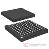
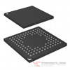
The STM32F103 is available in six different package options that accommodate diverse application requirements. The VFQFPN36 package provides a 6 by 6 millimeter footprint with 0.5 millimeter pitch, suitable for space-constrained applications. The LQFP48 package provides a 48-pin low-profile quad flat package for applications requiring moderate pin counts. The LQFP64 package provides 64 pins in a 10 by 10 millimeter footprint. The TFBGA64 package provides 64 pins in a 5 by 5 millimeter ball grid array for high-density applications. The LQFP100 package provides 100 pins in a 14 by 14 millimeter footprint for applications requiring maximum peripheral access. The LFBGA100 package provides 100 pins in a low-profile fine-pitch ball grid array for high-density applications.
The thermal resistance of each package varies based on its physical characteristics and heat dissipation capability. The LQFP100 package exhibits a junction-to-ambient thermal resistance of 46 degrees Celsius per watt under natural convection conditions. The TFBGA64 package exhibits a thermal resistance of 35 degrees Celsius per watt, providing improved heat dissipation compared to the LQFP packages due to its ball grid array construction.
The maximum junction temperature must not exceed 105 degrees Celsius for the extended temperature range variant or 85 degrees Celsius for the industrial temperature range variant. The junction temperature can be calculated from the ambient temperature, power dissipation, and package thermal resistance. Applications operating at high ambient temperatures or with significant power dissipation must select appropriate package options to maintain junction temperature within specified limits.
Electrical Characteristics and Operating Conditions of the STM32F103
The STM32F103 operates from a 2.0 to 3.6 volt power supply with specified electrical characteristics across this voltage range. The device maintains functionality across the full industrial temperature range from -40 to 85 degrees Celsius or the extended range from -40 to 105 degrees Celsius, depending on the selected variant.
The maximum current consumption in run mode depends on the operating frequency, code location, and peripheral configuration. At 72 megahertz with code executing from Flash memory and all peripherals disabled, the maximum current consumption is approximately 50 milliamperes. When code executes from SRAM, current consumption is reduced due to elimination of Flash memory access wait states. When peripherals are enabled, current consumption increases by approximately 0.8 milliamperes per enabled peripheral.
The sleep mode current consumption is reduced compared to run mode because the processor clock is halted while peripheral clocks continue operating. At 72 megahertz with peripherals disabled, sleep mode current consumption is approximately 20 milliamperes. The stop mode current consumption is further reduced to approximately 2 milliamperes when the voltage regulator operates in normal mode and approximately 0.5 milliamperes when the voltage regulator operates in low-power mode.
The standby mode current consumption is minimized to approximately 10 microamperes when the voltage regulator is disabled and the entire 1.8 volt domain is powered down. This extremely low standby current enables battery-powered applications to maintain operation for extended periods without requiring frequent battery replacement.
The ADC achieves 12-bit accuracy with typical integral nonlinearity of ±1.5 least significant bits and differential nonlinearity of ±1 least significant bit. The ADC accuracy is maintained across the full operating temperature range and supply voltage range when proper power supply decoupling is implemented.
The GPIO pins exhibit input high voltage thresholds of approximately 2.0 volts and input low voltage thresholds of approximately 0.8 volts, providing compatibility with both CMOS and TTL logic levels. The output high voltage is approximately 0.7 volts below the supply voltage when sourcing 8 milliamperes, and the output low voltage is approximately 0.4 volts when sinking 8 milliamperes.
Conclusion
The STM32F103 medium-density microcontroller family provides a comprehensive solution for applications requiring 32-bit processing capability with extensive peripheral integration. The combination of the ARM Cortex-M3 processor, multiple communication interfaces, analog-to-digital conversion, and flexible timing functions enables implementation of complex control and monitoring systems. The availability of multiple package options and memory densities allows designers to select the optimal configuration for their specific application requirements. The low-power operating modes and integrated power management features enable battery-powered applications to achieve extended operating life. The extensive debugging support and in-circuit programming capability facilitate rapid development and field updates. The STM32F103 represents a mature, well-established platform with extensive software support and development tools available from multiple vendors.
Frequently Asked Questions (FAQ)
- Q1. What is the maximum clock frequency achievable with the STM32F103, and how does it affect power consumption?
-
- A1. The STM32F103 achieves a maximum clock frequency of 72 megahertz when using an external high-speed crystal oscillator with the internal phase-locked loop. Power consumption increases approximately linearly with clock frequency, with typical current consumption increasing by approximately 0.7 milliamperes per 10 megahertz increase in clock frequency at 3.3 volts supply voltage. Applications can reduce power consumption by operating at lower clock frequencies when maximum performance is not required, with the internal 8 megahertz RC oscillator providing a low-power alternative to external oscillators.
- Q2. Can the STM32F103 operate from a single 3.3 volt power supply, or are multiple supply voltages required?
-
- A2. The STM32F103 can operate from a single 3.3 volt power supply, but the design incorporates separate analog and digital power pins to minimize noise coupling. The VDDA analog supply should be filtered separately from the VDD digital supply using a low-pass filter network. A maximum voltage difference of 300 millivolts between VDD and VDDA is tolerated. The VBAT pin can be connected to the same 3.3 volt supply or to a backup battery for real-time clock operation during main power loss.
- Q3. What is the conversion time for the analog-to-digital converters, and how many channels can be converted simultaneously?
-
- A3. The ADC achieves 1 microsecond conversion time when the ADC clock frequency is set to 14 megahertz. Each ADC can access up to 16 external analog input channels, and the two ADCs can operate simultaneously on different channels. The simultaneous sample-and-hold feature allows both ADCs to sample different analog inputs at precisely the same instant, enabling phase-accurate measurements of multiple signals. The scan mode allows sequential conversion of multiple channels with automatic channel switching between conversions.
- Q4. How long does it take for the STM32F103 to wake up from Stop mode, and what are the available wakeup sources?
-
- A4. The wakeup time from Stop mode depends on the clock source selected for resumption. When the internal 8 megahertz RC oscillator is used, wakeup occurs within approximately 5 microseconds. When an external oscillator is required, wakeup latency increases to accommodate oscillator startup time, typically ranging from 1 to 10 milliseconds. Available wakeup sources include any external interrupt line, the programmable voltage detector output, the real-time clock alarm, and the USB wakeup signal.
- Q5. What is the maximum current that can be sourced or sunk by a single GPIO pin, and what are the limitations on total I/O current?
-
- A5. Each GPIO pin can source or sink up to 8 milliamperes at nominal output levels, with relaxed output voltage specifications allowing up to 20 milliamperes sink current at reduced output voltage levels. The total current sourced by all GPIO pins plus the maximum run mode consumption cannot exceed the absolute maximum rating for total VDD current. Similarly, the total current sunk by all GPIO pins plus the maximum run mode consumption cannot exceed the absolute maximum rating for total VSS current. These limitations must be considered when designing applications with multiple high-current outputs.
- Q6. Can the STM32F103 be used in automotive applications, and what temperature range is recommended?
-
- A6. The STM32F103 is suitable for automotive peripheral applications but is not qualified for use in safety-critical automotive systems. The extended temperature range variant (-40 to 105 degrees Celsius) is recommended for automotive applications to accommodate the wider temperature extremes encountered in vehicle environments. The device must be mounted in a location where the junction temperature does not exceed the specified maximum, which may require thermal management considerations in high-dissipation applications.
- Q7. What is the Flash memory endurance, and how many erase/write cycles can be performed?
-
- A7. The Flash memory endurance is specified as 10,000 erase/write cycles minimum over the full temperature range. The Flash memory data retention is specified as 20 years at 55 degrees Celsius. These specifications ensure that the Flash memory can withstand typical application requirements for firmware updates and parameter storage. Applications requiring frequent Flash updates should implement wear-leveling algorithms to distribute erase cycles across multiple memory locations.
- Q8. How is the real-time clock powered when the main power supply is removed?
-
- A8. The real-time clock is powered through the VBAT pin, which can be connected to a backup battery or capacitor. When the main VDD supply is present, the VBAT supply is automatically selected through an internal power switch. When the main supply is removed, the VBAT supply maintains power to the real-time clock, backup registers, and the 32 kilohertz oscillator. The VBAT supply voltage range is 1.8 to 3.6 volts, allowing use of standard coin-cell batteries or supercapacitors.
- Q9. What debugging interfaces are supported, and can the device be programmed in-circuit?
-
- A9. The STM32F103 supports both JTAG and serial wire debug protocols through the combined Serial Wire JTAG Debug Port. The serial wire debug interface requires only two pins (SWDIO and SWCLK), simplifying board design compared to JTAG which requires four pins. In-circuit programming of the Flash memory is supported through the USART1 interface using a bootloader located in system memory. The bootloader is invoked by holding specific boot pins at defined logic levels during device reset, enabling field firmware updates without specialized programming equipment.
- Q10. What is the maximum I2C bus frequency, and are there any restrictions on external pull-up resistor values?
-
- A10. The I2C bus supports standard mode operation up to 100 kilohertz and fast mode operation up to 400 kilohertz. The maximum achievable I2C frequency depends on the external pull-up resistor values and the capacitive loading of the bus. For fast mode operation at 400 kilohertz, the external pull-up resistors should be in the range of 2 to 4 kiloohms. The PCLK1 frequency must be at least 2 megahertz for standard mode operation and at least 4 megahertz for fast mode operation.
- Q11. How many independent PWM outputs can be generated, and what is the maximum PWM frequency?
-
- A11. The STM32F103 can generate up to 12 independent PWM outputs: 6 from the advanced-control timer (TIM1) and up to 4 each from the three general-purpose timers (TIM2, TIM3, TIM4). The maximum PWM frequency depends on the timer clock frequency and the desired resolution. At 72 megahertz timer clock with 16-bit resolution, the maximum PWM frequency is approximately 1.1 kilohertz. Higher PWM frequencies can be achieved by reducing the resolution or using lower timer clock frequencies.
- Q12. What are the power supply decoupling requirements for proper ADC operation?
-
- A12. The ADC requires separate decoupling of the analog power supply (VDDA) from the digital power supply (VDD). A 10 nanofarad ceramic capacitor should be connected directly between VDDA and VSSA pins, placed as close as possible to the device pins. An additional 100 nanofarad ceramic capacitor should be connected between VDD and VSS pins. If the VREF+ pin is available (100-pin packages), a 10 nanofarad capacitor should be connected between VREF+ and VREF-. The capacitors should be high-quality ceramic types designed for high-frequency applications to minimize impedance at the ADC operating frequency.
- Q13. Can the STM32F103 interface with 5-volt logic circuits, or is level translation required?
-
- A13. Most GPIO pins on the STM32F103 are 5-volt tolerant, allowing direct connection to 5-volt logic circuits