Core Architecture and Processing Capabilities of the STM32F103
The STM32F103 employs the ARM Cortex-M3 core, a modern 32-bit processor architecture optimized for microcontroller applications. Operating at 72 MHz, the core delivers 1.25 DMIPS per megahertz at zero wait-state memory access, providing sufficient computational throughput for real-time signal processing and control tasks. The architecture includes single-cycle multiplication and hardware division capabilities, reducing execution time for mathematical operations commonly encountered in industrial applications.
The processor integrates a nested vectored interrupt controller (NVIC) capable of managing up to 43 maskable interrupt channels with 16 priority levels. This architecture enables low-latency interrupt processing through closely coupled NVIC core interface, allowing the processor to handle time-critical events with minimal overhead. The NVIC supports tail-chaining, a feature that permits processing of higher-priority interrupts arriving during lower-priority interrupt servicing, and automatic processor state saving and restoration, eliminating instruction overhead during context switching.
Memory Organization and Data Storage in the STM32F103
The STM32F103 implements a hierarchical memory architecture combining embedded Flash memory for program storage with SRAM for runtime data. The Flash memory capacity varies between 64 KB and 128 KB depending on the device variant, providing sufficient space for complex firmware implementations. The 20 KB of embedded SRAM operates at CPU clock speed with zero wait states, ensuring rapid data access during execution.
Beyond conventional memory, the STM32F103 incorporates a cyclic redundancy check (CRC) calculation unit for data integrity verification. This hardware block computes CRC signatures from 32-bit data words using a fixed generator polynomial, enabling runtime verification of Flash memory contents against reference signatures generated during compilation. This capability supports compliance with industrial safety standards such as EN/IEC 60335-1, which mandate periodic verification of program memory integrity.
The device also features backup registers—ten 16-bit registers providing 20 bytes of persistent storage—that retain data when the main power supply is absent, powered instead through a dedicated VBAT pin. This architecture enables applications to maintain critical state information across power cycles without external memory components.
Clock Management and Power Supply Architecture of the STM32F103
The STM32F103 incorporates a sophisticated clock distribution system supporting multiple clock sources and flexible frequency scaling. The system defaults to an internal 8 MHz RC oscillator upon reset, with provisions for switching to external clock sources ranging from 4 to 16 MHz. An integrated phase-locked loop (PLL) multiplies the input clock to achieve the maximum 72 MHz system frequency, with automatic clock failure detection that reverts to the internal oscillator if the external source becomes unstable.
The clock tree includes separate prescalers for the AHB bus (maximum 72 MHz), high-speed APB2 domain (maximum 72 MHz), and low-speed APB1 domain (maximum 36 MHz). This architecture permits independent frequency scaling of different functional blocks, enabling power optimization by reducing clock rates for peripherals not requiring maximum performance.
Power supply management incorporates integrated power-on reset (POR) and power-down reset (PDR) circuitry that maintains the device in reset state when supply voltage falls below 2 V, eliminating the need for external reset circuits. A programmable voltage detector (PVD) monitors supply voltage and generates interrupts when the supply approaches specified thresholds, enabling software to implement graceful shutdown procedures or activate backup power sources.
The device accepts supply voltages between 2.0 and 3.6 V, with separate analog supply pins (VDDA and VSSA) for the ADC and internal oscillator circuits. A dedicated VBAT pin supplies the real-time clock and backup registers when the main supply is absent, maintaining timekeeping and state information during power loss.
Low-Power Operating Modes and Energy Efficiency in the STM32F103
The STM32F103 implements three distinct low-power modes addressing different application requirements. Sleep mode halts the CPU while maintaining peripheral operation and clock distribution, permitting rapid wake-up through interrupt events with minimal latency. This mode reduces power consumption while preserving the ability to respond to external stimuli, making it suitable for applications requiring frequent brief processing bursts.
Stop mode achieves lower power consumption by disabling all clocks in the 1.8 V domain, including the PLL and both internal and external oscillators. The voltage regulator can operate in either normal or low-power mode during Stop, with the latter providing additional power reduction at the cost of slightly longer wake-up time. SRAM and register contents are preserved, enabling rapid resumption of execution. The device exits Stop mode through any external interrupt line, the programmable voltage detector output, the real-time clock alarm, or USB wake-up events.
Standby mode represents the lowest power consumption state, achieved by disabling the internal voltage regulator and powering down the entire 1.8 V domain. All oscillators are disabled, and SRAM contents are lost except for registers in the backup domain. The device exits Standby mode only through external reset, independent watchdog reset, a rising edge on the WKUP pin, or real-time clock alarm. This mode suits applications requiring extended periods of inactivity with periodic wake-up events.
Interrupt Handling and Event Management in the STM32F103
The STM32F103 incorporates an external interrupt/event controller (EXTI) providing 19 edge detector lines for generating interrupt or event requests. Each line can be independently configured to trigger on rising edges, falling edges, or both, with individual masking capability. This architecture permits detection of external signals with pulse widths shorter than the internal APB2 clock period, enabling reliable capture of brief transient events.
Up to 80 general-purpose I/O pins can be connected to 16 external interrupt lines through configurable port mapping, providing flexibility in circuit design. The EXTI maintains a pending register tracking interrupt request status, enabling software to determine which external events have occurred and require servicing.
Timer and Watchdog Functions in the STM32F103
The STM32F103 integrates seven timing functions addressing diverse application requirements. An advanced-control timer (TIM1) provides three-phase PWM generation with complementary outputs and programmable dead-time insertion, supporting motor control applications. This timer features four independent channels configurable for input capture, output compare, PWM generation in edge- or center-aligned modes, or one-pulse mode operation.
Three general-purpose timers (TIM2, TIM3, TIM4) provide 16-bit auto-reload up/down counters with 16-bit prescalers and four independent channels each. These timers support input capture, output compare, PWM generation, and one-pulse mode, with capability to handle quadrature encoder signals and hall-effect sensor outputs for motor feedback applications. All timers can be synchronized through the Timer Link feature for coordinated operation.
Two watchdog timers provide hardware-based system monitoring. The independent watchdog operates from a dedicated 40 kHz internal RC oscillator, functioning independently of the main clock and remaining active during Stop and Standby modes. The window watchdog operates from the main clock and provides early warning interrupt capability before device reset.
A 24-bit SysTick timer dedicated to operating system support includes autoreload capability and maskable interrupt generation, with programmable clock source selection.
Communication Interfaces Supported by the STM32F103
The STM32F103 provides comprehensive communication capabilities through multiple interface standards. Up to two I²C bus interfaces operate in multimaster and slave modes, supporting both standard and fast-mode speeds with dual slave addressing and 7/10-bit addressing in master mode. Hardware CRC generation and verification are embedded, with DMA support for efficient data transfer.
Three USART interfaces provide asynchronous serial communication at speeds up to 4.5 Mbit/s for one interface and 2.25 Mbit/s for the others. These interfaces include hardware CTS/RTS signal management, IrDA SIR ENDEC support, ISO 7816 compliance for smart card applications, and LIN master/slave capability. All USART interfaces support DMA-assisted data transfer.
Two SPI interfaces enable synchronous serial communication at speeds up to 18 Mbit/s in both master and slave modes, supporting full-duplex and simplex operation. The 3-bit prescaler provides eight selectable master mode frequencies, with configurable 8-bit or 16-bit frame sizes. Hardware CRC generation supports SD Card and MMC interface modes.
A CAN interface implements the CAN 2.0A and 2.0B (active) specifications with bit rates up to 1 Mbit/s, supporting both standard 11-bit and extended 29-bit identifiers. The interface includes three transmit mailboxes, two receive FIFOs with three stages, and 14 scalable filter banks for message filtering.
A USB 2.0 full-speed interface operates at 12 Mbit/s with software-configurable endpoint settings and suspend/resume support. The dedicated 48 MHz clock is generated from the internal PLL using an external high-speed crystal oscillator.
Analog Signal Processing with the STM32F103 ADC System
The STM32F103 incorporates two independent 12-bit analog-to-digital converters, each capable of processing up to 16 external analog input channels. The converters operate in single-shot or scan modes, with scan mode enabling automatic sequential conversion of selected channel groups. Simultaneous sample-and-hold, interleaved sample-and-hold, and single-shunt configurations provide flexibility for different measurement scenarios.
The ADC conversion range spans 0 to 3.6 V, with conversion time of approximately 1 microsecond achievable when the APB2 clock operates at 14 MHz, 28 MHz, or 56 MHz. An analog watchdog feature monitors converted voltage values against programmable thresholds, generating interrupts when measurements exceed specified bounds. This capability enables autonomous threshold detection without continuous software polling.
The ADC system includes an internal temperature sensor connected to ADC channel 16, providing temperature measurement capability for thermal monitoring applications. The sensor generates a voltage that varies linearly with temperature, enabling firmware to implement temperature-based control logic or thermal shutdown procedures.
General-Purpose Input/Output Configuration in the STM32F103
The STM32F103 provides up to 80 general-purpose I/O pins depending on package selection, with each pin individually configurable as input, output, or peripheral alternate function. Output pins support push-pull or open-drain configurations, while input pins can include pull-up or pull-down resistors. Most GPIO pins are 5 V tolerant, enabling direct interface with legacy 5 V logic systems.
GPIO pins on the APB2 bus support toggling speeds up to 18 MHz, with output drive capability of ±8 mA in standard mode or ±20 mA in relaxed mode. The I/O alternate function configuration can be locked through a specific software sequence to prevent accidental modification of pin assignments during runtime.
Electrical Characteristics and Operating Conditions of the STM32F103
The STM32F103 operates across ambient temperatures from -40°C to +85°C (industrial range) or -40°C to +105°C (extended range), with junction temperature limits of 105°C and 125°C respectively. Supply voltage tolerance spans 2.0 to 3.6 V, with separate analog supply pins requiring minimum 2.4 V when the ADC is active.
Maximum current consumption in Run mode at 72 MHz and 3.6 V supply reaches approximately 50 mA with all peripherals enabled. Sleep mode reduces consumption to approximately 20 mA, while Stop mode with regulator in low-power mode achieves approximately 2 mA. Standby mode consumption drops to approximately 10 microamperes, enabling extended battery operation for applications with infrequent wake-up requirements.
The device implements comprehensive electrostatic discharge (ESD) protection with absolute maximum ratings of 2 kV for human body model and 200 V for machine model testing. Electromagnetic susceptibility testing confirms functional operation under industrial electromagnetic environments, with specific immunity levels documented for ESD, fast transient burst, and other interference sources.
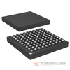
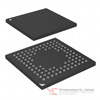
Package Options and Thermal Management for the STM32F103
The STM32F103 is available in six package options accommodating different circuit board space and pin count requirements. The VFQFPN36 package provides 36 pins in a 6×6 mm footprint with 0.5 mm pitch, suitable for space-constrained applications. The LQFP48 and LQFP64 packages offer 48 and 64 pins respectively in quad flat pack format with 0.5 mm pitch.
The LQFP100 package provides 100 pins in quad flat pack format, offering maximum peripheral access. The LFBGA100 and TFBGA64 ball grid array packages provide alternative high-density interconnection options with 0.75 mm and 0.5 mm pitch respectively.
Thermal management requires consideration of junction-to-ambient thermal resistance, which varies from 46°C/W for LQFP100 to 81°C/W for VFQFPN36. Maximum junction temperature must remain below 105°C or 125°C depending on temperature range selection. Thermal calculations should account for both internal power dissipation (product of supply current and voltage) and I/O power dissipation (sum of output pin power contributions).
Conclusion
The STM32F103 medium-density microcontroller family delivers a comprehensive embedded processing solution combining the ARM Cortex-M3 core with extensive peripheral integration, flexible clock management, and sophisticated power control. The dual ADC system, multiple communication interfaces, and comprehensive timer functions address the requirements of industrial control, motor drive, medical equipment, and consumer electronics applications. The availability of multiple package options and temperature ranges enables designers to select configurations matching specific application constraints. The integration of hardware watchdog timers, CRC calculation, and programmable voltage detection supports implementation of robust, reliable systems suitable for demanding industrial environments.
Frequently Asked Questions (FAQ)
- Q1. What is the maximum operating frequency of the STM32F103, and how does it affect power consumption?
-
- A1. The STM32F103 operates at a maximum frequency of 72 MHz. Power consumption increases approximately linearly with operating frequency due to increased switching activity in the processor and peripherals. At 72 MHz with all peripherals enabled, typical current consumption reaches approximately 50 mA at 3.6 V supply. Reducing the operating frequency through clock prescaling provides proportional power reduction, enabling designers to optimize performance versus power consumption based on application requirements.
- Q2. How many communication interfaces does the STM32F103 provide, and which applications benefit most from this integration?
-
- A2. The STM32F103 integrates up to nine communication interfaces: two I²C buses, three USARTs, two SPIs, one CAN interface, and one USB 2.0 full-speed interface. This comprehensive integration benefits applications requiring simultaneous communication with multiple external systems—for example, industrial equipment that must communicate with sensors via I²C, transmit data to a host computer via USART, and participate in a vehicle network via CAN. The integration reduces component count and simplifies circuit design compared to systems requiring separate communication controllers.
- Q3. What is the purpose of the backup domain and VBAT pin in the STM32F103?
-
- A3. The backup domain, powered through the VBAT pin, maintains the real-time clock and ten 16-bit backup registers when the main power supply is absent. This architecture enables applications to preserve critical state information and maintain accurate timekeeping across power cycles without requiring external battery-backed memory. The backup registers can store 20 bytes of application data, sufficient for storing configuration parameters, system state flags, or calibration values that must survive power loss.
- Q4. How does the STM32F103 handle external clock failure, and why is this feature important?
-
- A4. The STM32F103 monitors the external high-speed clock source for failure and automatically switches to the internal 8 MHz RC oscillator if the external clock becomes unstable. A software interrupt is generated when this automatic switchover occurs, enabling firmware to log the failure event and implement appropriate recovery procedures. This feature prevents system lockup in applications where external clock failure might otherwise halt processor operation, improving system reliability in environments subject to electromagnetic interference or component failures.
- Q5. What are the differences between Sleep, Stop, and Standby modes, and how should designers select between them?
-
- A5. Sleep mode halts the CPU while maintaining peripheral operation and clock distribution, reducing power consumption to approximately 20 mA while enabling rapid wake-up through interrupts. Stop mode disables all clocks in the 1.8 V domain, achieving approximately 2 mA consumption while preserving SRAM and register contents. Standby mode disables the voltage regulator entirely, achieving approximately 10 microamperes consumption but losing SRAM contents except for backup registers. Designers should select Sleep mode for applications requiring frequent brief processing bursts, Stop mode for applications with periodic wake-up events where SRAM preservation is important, and Standby mode for applications with extended inactivity periods where minimal power consumption is paramount.
- Q6. What is the resolution and conversion time of the STM32F103 ADC system?
-
- A6. The STM32F103 incorporates two independent 12-bit analog-to-digital converters with conversion time of approximately 1 microsecond. This conversion time is achievable when the APB2 clock operates at 14 MHz, 28 MHz, or 56 MHz. The 12-bit resolution provides 4096 discrete levels across the 0 to 3.6 V input range, delivering approximately 0.88 mV per least significant bit. The dual ADC architecture enables simultaneous sampling of two channels or interleaved sampling for increased effective sampling rate.
- Q7. How many external interrupt lines does the STM32F103 support, and what is the maximum number of GPIO pins that can be connected to these lines?
-
- A7. The STM32F103 provides 19 edge detector lines in the external interrupt/event controller, with 16 of these lines available for connection to general-purpose I/O pins. Up to 80 GPIO pins can be connected to these 16 external interrupt lines through configurable port mapping, enabling flexible circuit design. Each interrupt line can be independently configured to trigger on rising edges, falling edges, or both, with individual masking capability.
- Q8. What timer options are available in the STM32F103, and which applications require the advanced-control timer?
-
- A8. The STM32F103 provides seven timing functions: one advanced-control timer (TIM1), three general-purpose timers (TIM2-TIM4), two watchdog timers, and one SysTick timer. The advanced-control timer provides three-phase PWM generation with complementary outputs and programmable dead-time insertion, making it essential for motor control applications requiring precise switching control. General-purpose timers suit applications requiring basic timing, pulse counting, or PWM generation without the complexity of three-phase motor control.
- Q9. What is the CRC calculation unit, and how does it support system reliability?
-
- A9. The CRC calculation unit computes cyclic redundancy check signatures from 32-bit data words using a fixed generator polynomial. This hardware block enables runtime verification of Flash memory contents against reference signatures generated during compilation, supporting compliance with industrial safety standards such as EN/IEC 60335-1. The CRC calculation can be performed periodically during operation to detect memory corruption caused by radiation, electromagnetic interference, or component degradation, enabling firmware to implement appropriate error recovery procedures.
- Q10. How should designers select between the STM32F103x8 (64 KB Flash) and STM32F103xB (128 KB Flash) variants?
-
- A10. The selection between STM32F103x8 and STM32F103xB depends on firmware size requirements. The STM32F103x8 provides 64 KB of Flash memory suitable for applications with moderate firmware complexity, while the STM32F103xB provides 128 KB for applications requiring extensive firmware functionality, large lookup tables, or multiple firmware versions. Both variants share identical peripheral integration and performance characteristics, enabling designers to select the appropriate memory density based on application requirements without affecting other system aspects.
- Q11. What package options are available for the STM32F103, and how do they differ in terms of pin count and physical size?
-
- A11. The STM32F103 is available in six packages: VFQFPN36 (36 pins, 6×6 mm), LQFP48 (48 pins), LQFP64 (64 pins), TFBGA64 (64 pins, ball grid array), LQFP100 (100 pins), and LFBGA100 (100 pins, ball grid array). The VFQFPN36 provides the smallest footprint for space-constrained applications, while LQFP100 and LFBGA100 provide maximum peripheral access. Ball grid array packages offer superior thermal performance and reduced electromagnetic emissions compared to quad flat pack alternatives, making them suitable for high-performance applications.
- Q12. What are the power supply requirements for the STM32F103, and how should designers implement power distribution?
-
- A12. The STM32F103 requires main supply voltage (VDD) between 2.0 and 3.6 V, with separate analog supply pins (VDDA and VSSA) for the ADC and internal oscillator circuits. The analog supply must maintain minimum 2.4 V when the ADC is active. A dedicated VBAT pin supplies the real-time clock and backup registers when main power is absent. Designers should implement separate power distribution networks for analog and digital supplies, with 10 nF ceramic decoupling capacitors placed as close as possible to each supply pin. The analog supply should be filtered with additional LC filtering to minimize noise affecting ADC accuracy.