STM32H743VIT6 Product Overview
The STM32H743VIT6 is a member of the STM32H743xI/G and STM32H7 family from STMicroelectronics. It is a 32-bit microcontroller built around an Arm Cortex-M7 core and positioned for applications that need high clock frequency, substantial on-chip memory, broad peripheral integration, and support for both digital control and analog interfacing.
In this specific variant, the STM32H743VIT6 combines a single-core 32-bit Arm Cortex-M7 CPU running at up to 480 MHz with 2 MB of embedded flash memory and up to 1 MB of RAM within the STM32H743xI/G device family. The device is offered in a 100-pin LQFP package with 82 I/O lines available, making it suitable for designs that need both processing density and a substantial number of external connections in a moderate package size.
The datasheet identifies the STM32H743xI/G and STM32H742xI/G devices as 480 MHz MCUs with up to 2 MB flash, up to 1 MB RAM, and up to 46 communication and analog interfaces. The STM32H743VIT6 specifically operates over a 1.71 V to 3.6 V supply range, integrates 36 channels of 16-bit ADC capability and two 12-bit DACs, and supports an operating ambient temperature range of -40°C to 85°C.
From a functional standpoint, the STM32H743VIT6 is organized to combine high-performance computation, layered memory access, broad communication support, hardware acceleration blocks, extensive timer resources, and multiple power domains. That combination allows one device to support tasks such as control loops, signal acquisition, graphical output, communication gateway functions, and data buffering without requiring many external support ICs.
STM32H743VIT6 Core Architecture and Performance Capabilities
At the center of the STM32H743VIT6 is the 32-bit Arm Cortex-M7 core with double-precision floating-point unit, DSP instructions, and L1 cache consisting of 16 KB instruction cache and 16 KB data cache. The device reaches up to 480 MHz and is specified at 1027 DMIPS, corresponding to 2.14 DMIPS/MHz based on Dhrystone 2.1.
This processing structure places the STM32H743VIT6 in the category of microcontrollers intended for workloads beyond basic control and monitoring. The combination of high clock frequency, floating-point support, and DSP instructions means the device can execute operations such as digital filtering, motor control computation, waveform analysis, sensor fusion, and protocol handling with reduced software overhead compared with lower-end MCU cores.
The STM32H743VIT6 also includes an MPU, or memory protection unit. In practical use, an MPU helps segment software regions and define access rules, which supports more structured firmware architectures. For example, a design can separate a communication stack, motor-control algorithm, and graphical interface into distinct memory areas with controlled privileges, reducing unintended memory access between tasks.
The internal organization is also split into multiple domains: D1 for high-performance capabilities, D2 for communication peripherals and timers, and D3 for reset, clock control, and power management. This domain-based architecture is not just a layout detail. It supports more selective clocking and power behavior, so parts of the chip can remain active while others are gated or switched off according to the application state.
STM32H743VIT6 Memory Architecture and Data Handling Resources
The STM32H743VIT6 provides up to 2 MB of flash memory with read-while-write support. This characteristic is useful in applications where firmware needs to continue executing while another flash area is being updated, logged, or reprogrammed. It can simplify field-update strategies and nonvolatile data handling.
The RAM resources in the STM32H743xI/G family reach up to 1 MB. The datasheet breaks this into several blocks, including 192 KB of TCM RAM, made up of 64 KB ITCM RAM and 128 KB DTCM RAM, up to 864 KB of user SRAM, and 4 KB of SRAM in the backup domain.
This partitioning matters because the memory types are intended for different access patterns. ITCM and DTCM are suited to time-critical code and data. User SRAM supports more general-purpose buffering and application data storage. Backup SRAM remains available in the backup domain for retention-oriented functions tied to RTC or VBAT-backed operation.
The STM32H743VIT6 also supports a flexible external memory controller with up to a 32-bit data bus for SRAM, PSRAM, SDRAM, LPSDR SDRAM, and NOR/NAND flash, with synchronous memory clocked up to 100 MHz. In addition, it integrates a dual-mode Quad-SPI memory interface running up to 133 MHz. Together, these interfaces allow the STM32H743VIT6 to scale beyond its internal memory capacity when an application requires larger frame buffers, external code storage, or high-speed data logging.
A practical example is a system that collects image data through the camera interface while also driving a display. Internal SRAM can hold intermediate data structures and real-time control variables, while external SDRAM can store larger image buffers, and Quad-SPI flash can contain fonts, graphics, or expanded firmware assets.
DMA support further shapes data handling performance. The STM32H743VIT6 includes four DMA controllers: one high-speed master DMA with linked-list support, two dual-port DMAs with FIFO, and one basic DMA with request router capabilities. These controllers reduce CPU involvement in routine memory transfers, improving throughput for display refresh, ADC sampling, communication streams, and memory-to-memory movement.
STM32H743VIT6 Power Supply Scheme, Reset Control, and Low-Power Operation
The STM32H743VIT6 operates from a 1.62 V to 3.6 V application supply and I/O range at the family level, while the provided product summary for this variant lists 1.71 V to 3.6 V. The device integrates power supervision features including POR, PDR, PVD, and BOR. These functions monitor supply conditions during startup and operation and help maintain predictable reset behavior when voltage conditions move outside valid ranges.
The device uses an embedded LDO regulator with configurable and scalable output to supply the digital circuitry. It also supports voltage scaling in Run and Stop modes across six configurable ranges. This allows firmware to balance frequency and power behavior according to workload conditions.
The STM32H743VIT6 also includes a dedicated USB power feature embedding a 3.3 V internal regulator to supply the internal PHYs. For designs using USB functionality, this reduces the need for separate external support for that internal power domain.
Three separate power domains are provided. These can be independently clock-gated or switched off:
D1 for high-performance functions,
D2 for communication peripherals and timers,
D3 for reset, clock, and power management.
This domain-level power structure allows application-specific sleep strategies. For instance, a design may stop the high-performance processing domain while retaining selected communication or RTC functions in another domain.
The STM32H743VIT6 supports low-power modes including Sleep, Stop, Standby, and VBAT mode with battery charging support. The datasheet lists standby current as 2.95 µA with Backup SRAM off and RTC/LSE on. It also includes a backup regulator around 0.9 V and 4 KB backup SRAM in the backup domain.
VBAT battery operating mode allows the backup section to remain alive when the main supply is removed. This can preserve RTC operation and retained values such as timestamp information, boot counters, alarm settings, or last-state markers.
STM32H743VIT6 Clock System and Internal Device Organization
Clocking flexibility is a major part of the STM32H743VIT6 architecture. The device integrates multiple internal oscillators:
64 MHz HSI,
48 MHz HSI48,
4 MHz CSI,
32 kHz LSI.
It also supports external oscillators:
4 MHz to 48 MHz HSE,
32.768 kHz LSE.
Three PLLs are included, one for the system clock and two for kernel clocks, with fractional mode support. This arrangement allows different subsystems to receive clocks tailored to their requirements. A communication interface can run from its own kernel clock while the core and memory bus operate at a different frequency relationship.
The bus organization includes three bus matrices, one AXI and two AHB, along with bridges between domains and peripheral buses. This layered bus structure supports high-bandwidth data movement between core, memory, DMA engines, and peripherals.
In practice, this means the STM32H743VIT6 is arranged less like a simple MCU with one CPU and one peripheral bus, and more like a compact embedded computing platform with multiple concurrent traffic paths. That becomes relevant when several functions run at once, such as Ethernet transfers, display updates, ADC acquisition, and application code execution.
STM32H743VIT6 GPIO, Interrupt Structure, and System Control Functions
The STM32H743VIT6 provides up to 168 I/O ports at the family level, while the STM32H743VIT6 package configuration provides 82 I/O lines. These I/Os support interrupt capability and extensive alternate functions for communication, timing, memory bus access, and display or imaging connectivity.
The interrupt architecture includes the NVIC and EXTI blocks. NVIC provides the nested vectored interrupt controller for managing prioritized interrupt service execution, while EXTI extends event and interrupt handling to external sources. This arrangement lets the device handle a mix of fast internal events and pin-driven responses.
A CRC calculation unit is also included. CRC hardware is often used to verify communication frames, stored configuration blocks, or firmware images. Offloading such calculations to hardware reduces CPU cycles in systems that frequently validate data blocks.
Reset handling is managed through the reset and clock controller, which also centralizes system reset sources. In firmware design, this helps create traceable startup behavior because software can distinguish or respond to different reset causes such as power-on, watchdog, or software-triggered reset.
STM32H743VIT6 Analog Integration and Signal Processing Functions
The STM32H743VIT6 integrates an extensive analog subsystem. It provides three ADCs with up to 16-bit resolution, supporting up to 36 channels and up to 3.6 MSPS. It also includes one temperature sensor, two 12-bit DACs operating at 1 MHz, two ultra-low-power comparators, two operational amplifiers with 7.3 MHz bandwidth, and one DFSDM block with 8 channels and 4 filters.
The ADC resources make the STM32H743VIT6 suitable for multi-channel acquisition systems where several analog inputs must be sampled at moderate to high precision. Examples include current and voltage monitoring, pressure or position sensing, mixed industrial inputs, or synchronized multi-channel measurement.
The integrated DACs can generate analog output waveforms, threshold references, or control voltages. In a control system, one DAC might create a reference signal for an external stage while the ADCs measure the resulting feedback path.
Comparators and operational amplifiers add more analog front-end flexibility. Rather than requiring separate external analog devices in every design, the STM32H743VIT6 can absorb some conditioning and threshold-detection functions on chip. This can simplify the BOM in systems where moderate analog integration is enough.
The DFSDM block is useful when working with sigma-delta modulators and digital filtering chains. That broadens the STM32H743VIT6 beyond conventional MCU ADC-only use cases and makes it more suitable for designs needing digital conversion pipelines with filtering.
The device also includes voltage reference support for analog peripherals through VREF+, along with characteristics defined in the electrical sections for embedded reference voltage and calibration values.
STM32H743VIT6 Timers, Watchdogs, RTC, and Control-Oriented Peripheral Resources
The STM32H743VIT6 includes up to 22 timers and watchdogs. These are not uniform timers; the set includes specialized blocks for high-resolution control, motor control, general timing, low-power timing, and system supervision.
The timer resources include:
1 high-resolution timer with up to 2.1 ns maximum resolution,
2 32-bit timers with up to 4 input capture, output compare, PWM, pulse counter, and quadrature encoder capability up to 240 MHz,
2 16-bit advanced motor-control timers up to 240 MHz,
10 16-bit general-purpose timers up to 240 MHz,
5 16-bit low-power timers up to 240 MHz,
2 watchdogs,
1 SysTick timer.
The high-resolution timer is suited to power conversion or precision waveform generation where sub-microsecond timing granularity is needed. The advanced-control timers align with motor-control applications, especially where complementary outputs, PWM generation, and synchronized timing behavior are required.
The 32-bit timers with quadrature encoder support can directly serve motion-related applications such as rotary position tracking. For instance, in a servo system, one timer may decode an encoder while another generates PWM, with ADC sampling synchronized to the control cycle.
The independent watchdog and window watchdog provide two layers of software supervision. The RTC includes sub-second accuracy and a hardware calendar, supported by the backup domain. Together with backup SRAM and backup registers, this makes the STM32H743VIT6 suitable for systems that need persistent timekeeping and retained state across resets or main power interruptions.
STM32H743VIT6 Communication Interfaces and External Connectivity
Connectivity is one of the defining characteristics of the STM32H743VIT6. The STM32H743xI/G family provides up to 35 communication peripherals, giving the device the flexibility to act as a controller, gateway, node, or mixed-interface endpoint.
The communication set includes:
4 I2C FM+ interfaces with SMBus/PMBus support,
4 USARTs and 4 UARTs with features including ISO7816, LIN, IrDA, and data rates up to 12.5 Mbit/s, plus 1 LPUART,
6 SPIs, with 3 supporting muxed duplex I2S audio class operation up to 150 MHz,
4 SAIs,
1 SPDIFRX receiver,
1 SWPMI interface,
MDIO slave interface,
2 SD/SDIO/MMC interfaces up to 125 MHz,
2 CAN controllers with CAN FD and one with TT-CAN,
2 USB OTG interfaces, one FS and one HS/FS,
Ethernet MAC with DMA controller,
HDMI-CEC,
8- to 14-bit camera interface up to 80 MHz.
This range allows the STM32H743VIT6 to connect to legacy serial devices, modern CAN FD networks, Ethernet-based systems, USB peripherals, memory cards, audio interfaces, and image sensors. A single design can therefore combine local sensing, network connection, removable storage, and user-interface hardware around one MCU.
For example, an embedded HMI controller could use Ethernet for network communication, SDMMC for local logging, LTDC for the display, DCMI for image capture, USB for maintenance access, and CAN FD for control network attachment, all on the same STM32H743VIT6.
The presence of DMA on major interfaces improves sustained transfer capability. In data-intensive applications, this lets the device move packets, frames, or sample streams with lower CPU interruption frequency.
STM32H743VIT6 Graphics, Display, Imaging, and Hardware Acceleration Features
The STM32H743VIT6 includes several hardware blocks that support graphics and imaging applications. These include an LCD-TFT controller up to XGA resolution, the Chrom-ART graphical hardware accelerator (DMA2D), a hardware JPEG codec, and a digital camera interface supporting 8- to 14-bit input up to 80 MHz.
The LCD-TFT controller allows direct management of display panels. The Chrom-ART accelerator reduces CPU load in graphics tasks such as image copying, color format conversion, and graphical composition. The hardware JPEG codec further offloads image compression or decompression processing.
In practical terms, this means the STM32H743VIT6 can support embedded display systems with more fluid interface behavior than a CPU-only graphics pipeline. If a system needs to capture an image from a camera, process or compress it, and display results on a TFT panel, the dedicated hardware blocks help divide that workload.
The digital camera interface complements the display and memory resources. Combined with external SDRAM through FMC and image storage through SDMMC or Quad-SPI, the STM32H743VIT6 can support compact imaging pipelines without requiring a separate application processor.
STM32H743VIT6 Package, Operating Range, and Electrical Characteristics Snapshot
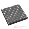
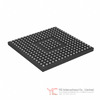
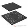
The STM32H743VIT6 is supplied in a 100-pin LQFP package with a 14 × 14 mm body. The package style is surface-mount and corresponds to the 100-LQFP supplier package listed for the product.
For environmental and regulatory classification, the device is listed as RoHS3 compliant and REACH unaffected, with moisture sensitivity level MSL 3 at 168 hours.
The operating ambient temperature range listed for the STM32H743VIT6 is -40°C to 85°C. The supply voltage range in the provided product data is 1.71 V to 3.6 V, while the broader family feature description notes 1.62 V to 3.6 V application supply and I/Os. Design work should therefore follow the exact conditions and revision-specific electrical characteristics applicable to the selected device revision.
The datasheet includes detailed electrical characteristics for different revisions, covering:
absolute maximum ratings,
general operating conditions,
VCAP operating conditions,
power-up and power-down behavior,
reset and power control block characteristics,
reference voltage characteristics,
supply current in Run, Sleep, Stop, Standby, and VBAT modes,
wake-up timing,
internal and external clock source characteristics,
PLL behavior,
memory characteristics,
EMC characteristics,
I/O characteristics,
FMC and Quad-SPI interface characteristics,
ADC, DAC, comparator, op amp, DFSDM, DCMI, LTDC, timer, and communication interface characteristics.
This breadth of characterization is useful because the STM32H743VIT6 is often used in systems where multiple subsystems interact. A design may need to confirm not only CPU speed and memory size, but also ADC timing, display timing, wake-up latency, bus timing for external memory, and current consumption under specific execution conditions such as running code from ITCM versus flash with cache enabled.
Conclusion
The STM32H743VIT6 from STMicroelectronics is a high-performance STM32H7 microcontroller built around a 480 MHz Arm Cortex-M7 core and backed by 2 MB of flash, up to 1 MB of RAM, broad timer resources, extensive communication interfaces, integrated analog capability, and dedicated graphics and imaging acceleration blocks.
Its architecture combines high-speed processing with segmented memory, DMA-rich data movement, multiple power domains, flexible clocking, and support for external memory expansion. That makes the STM32H743VIT6 suitable for designs that consolidate control, connectivity, signal acquisition, user interface, and data handling within one MCU platform.
The device stands out not by one isolated specification, but by how its CPU, memory hierarchy, analog subsystem, communication set, and hardware accelerators are arranged to support complex embedded systems with varied real-time demands.
Frequently Asked Questions (FAQ)
- Q1. What processor core does the STM32H743VIT6 use?
-
- A1. The STM32H743VIT6 uses a 32-bit Arm Cortex-M7 core. It includes a double-precision floating-point unit, DSP instructions, and L1 cache with 16 KB instruction cache and 16 KB data cache.
- Q2. What is the maximum operating frequency of the STM32H743VIT6?
-
- A2. The STM32H743VIT6 runs at up to 480 MHz.
- Q3. How much flash memory does the STM32H743VIT6 provide?
-
- A3. The STM32H743VIT6 provides 2 MB of embedded flash memory with read-while-write support.
- Q4. How much RAM is available in the STM32H743VIT6 family architecture?
-
- A4. The STM32H743xI/G family provides up to 1 MB of RAM, including 64 KB ITCM RAM, 128 KB DTCM RAM, up to 864 KB user SRAM, and 4 KB backup SRAM.
- Q5. What package does the STM32H743VIT6 use?
-
- A5. The STM32H743VIT6 is supplied in a 100-pin LQFP package with a 14 × 14 mm body.
- Q6. How many GPIOs are available on the STM32H743VIT6?
-
- A6. The product listing specifies 82 I/O lines for the STM32H743VIT6 package option.
- Q7. What supply voltage range does the STM32H743VIT6 support?
-
- A7. The provided product summary lists a supply range of 1.71 V to 3.6 V. The broader family description notes 1.62 V to 3.6 V for application supply and I/Os, so the applicable device revision and electrical conditions should be checked during design.
- Q8. What temperature range does the STM32H743VIT6 support?
-
- A8. The STM32H743VIT6 is listed for operation from -40°C to 85°C ambient temperature.
- Q9. Does the STM32H743VIT6 include ADCs?
-
- A9. Yes. The STM32H743VIT6 family includes 3 ADCs with up to 16-bit resolution, up to 36 channels, and sampling performance up to 3.6 MSPS.
- Q10. Does the STM32H743VIT6 include DACs?
-
- A10. Yes. It includes 2 DACs with 12-bit resolution and 1 MHz operation.
- Q11. What analog support blocks are integrated into the STM32H743VIT6 besides ADC and DAC?
-
- A11. The device includes a temperature sensor, 2 ultra-low-power comparators, 2 operational amplifiers with 7.3 MHz bandwidth, and 1 DFSDM block with 8 channels and 4 filters.
- Q12. Is the STM32H743VIT6 suitable for motor control or precision timing tasks?
-
- A12. The hardware resources support that type of use. The device includes 2 advanced motor-control timers, a high-resolution timer with up to 2.1 ns maximum resolution, general-purpose timers, low-power timers, and encoder-capable 32-bit timers.
- Q13. How many timers does the STM32H743VIT6 provide?
-
- A13. The STM32H743VIT6 family includes up to 22 timers and watchdogs, including high-resolution, advanced-control, general-purpose, low-power, watchdog, and SysTick timer resources.
- Q14. Does the STM32H743VIT6 support external memory?
-
- A14. Yes. It includes a flexible memory controller supporting SRAM, PSRAM, SDRAM, LPSDR SDRAM, and NOR/NAND flash with up to a 32-bit data bus, plus a Quad-SPI interface running up to 133 MHz.
- Q15. Can the STM32H743VIT6 be used with external SDRAM for frame buffers?
-
- A15. The hardware supports that approach through the flexible memory controller, which can interface with SDRAM and LPSDR SDRAM. This is useful for applications such as displays, image buffering, or large data structures.
- Q16. What DMA resources are available in the STM32H743VIT6?
-
- A16. The device includes 4 DMA controllers: 1 high-speed master DMA with linked-list support, 2 dual-port DMAs with FIFO, and 1 basic DMA with request router capabilities.
- Q17. Does the STM32H743VIT6 support Ethernet?
-
- A17. Yes. The STM32H743VIT6 includes an Ethernet MAC interface with a dedicated DMA controller.
- Q18. Does the STM32H743VIT6 support USB?
-
- A18. Yes. It provides 2 USB OTG interfaces: one full-speed interface and one high-speed/full-speed interface.
- Q19. What serial communication interfaces are available on the STM32H743VIT6?
-
- A19. The family includes 4 I2C interfaces, 4 USARTs, 4 UARTs, 1 LPUART, 6 SPI interfaces, 3 I2S-capable SPI instances, 4 SAI interfaces, SPDIFRX, SWPMI, MDIO slave, 2 SDMMC interfaces, and CAN controllers with CAN FD support.
- Q20. Does the STM32H743VIT6 support CAN FD?
-
- A20. Yes. The family includes 2 CAN controllers with CAN FD support, and one includes time-triggered CAN capability.
- Q21. Can the STM32H743VIT6 drive a display directly?
-
- A21. Yes. The STM32H743VIT6 family includes an LCD-TFT controller supporting up to XGA resolution.
- Q22. Does the STM32H743VIT6 include graphics acceleration?
-
- A22. Yes. It includes the Chrom-ART graphical hardware accelerator, also referred to as DMA2D, which reduces CPU load in graphics operations.
- Q23. Is JPEG hardware available in the STM32H743VIT6?
-
- A23. Yes. The device includes a hardware JPEG codec.
- Q24. Can the STM32H743VIT6 interface with a camera sensor?
-
- A24. Yes. It includes an 8- to 14-bit digital camera interface supporting up to 80 MHz input.
- Q25. What low-power modes are supported by the STM32H743VIT6?
-
- A25. The STM32H743VIT6 supports Sleep, Stop, Standby, and VBAT modes. It also includes backup domain resources and battery-related support.
- Q26. What standby current is specified for the STM32H743VIT6 family?
-
- A26. The datasheet cites 2.95 µA in Standby mode with Backup SRAM off and RTC/LSE on.
- Q27. Does the STM32H743VIT6 include RTC and backup memory?
-
- A27. Yes. The device includes an RTC with sub-second accuracy and hardware calendar, along with backup SRAM and backup registers in the backup domain.
- Q28. What clock sources are available in the STM32H743VIT6?
-
- A28. Internal clock sources include 64 MHz HSI, 48 MHz HSI48, 4 MHz CSI, and 32 kHz LSI. External clock sources include 4 MHz to 48 MHz HSE and 32.768 kHz LSE.
- Q29. How many PLLs are integrated into the STM32H743VIT6?
-
- A29. The device includes 3 PLLs: one for the system clock and two for kernel clocks, with fractional mode support.
- Q30. Does the STM32H743VIT6 include hardware support for debugging?
-
- A30. Yes. It provides SWD and JTAG interfaces, as well as a 4 KB embedded trace buffer.
- Q31. What safety or integrity-related monitoring functions are present in the STM32H743VIT6?
-
- A31. The device includes reset and supply supervision features such as POR, PDR, PVD, and BOR, along with CPU and domain power state monitoring pins, watchdog timers, CRC calculation hardware, and security features including ROP, PC-ROP, and active tamper.
- Q32. Does the STM32H743VIT6 provide a unique device identifier?
-
- A32. Yes. The STM32H743VIT6 family includes a 96-bit unique ID.
- Q33. Is the STM32H743VIT6 compliant with RoHS requirements?
-
- A33. Yes. The device is listed as RoHS3 compliant.
- Q34. What is the moisture sensitivity level of the STM32H743VIT6?
-
- A34. The listed moisture sensitivity level is MSL 3, with 168 hours.
- Q35. In what kind of system does the STM32H743VIT6 architecture make sense?
-
- A35. Based on its documented resources, the STM32H743VIT6 fits systems that combine high-speed processing, multiple communication links, analog measurement, timing control, display handling, or image-related functions in one microcontroller design.