Product overview of STM32H743VIH6
STM32H743VIH6 is a member of the STM32H7 series from STMicroelectronics, integrating a 32‑bit Arm Cortex‑M7 core running up to 480 MHz with double‑precision FPU and DSP instruction support. Positioned in the STM32H743xI/G family, it combines up to 2 MB of embedded flash and up to 1 MB of RAM with a dense set of digital, analog, connectivity, graphics and security functions.
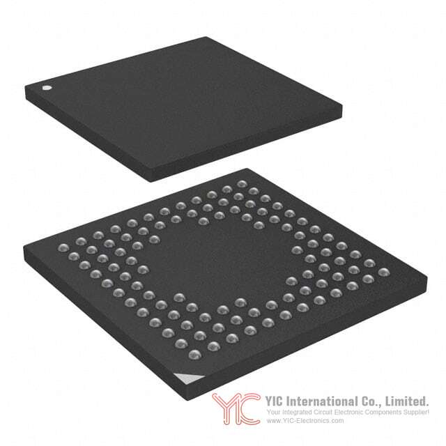
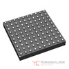
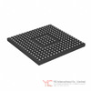
The STM32H743VIH6 is delivered in a 100‑pin TFBGA (8 × 8 mm) package and supports a supply voltage range of 1.62 V to 3.6 V for both core supply (through internal regulation) and I/Os. Operating temperature spans -40 °C to 85 °C (TA). The device includes 82 general‑purpose I/O lines, three ADCs, DACs, multiple timers, a flexible memory controller, dual‑mode Quad‑SPI, USB OTG (FS and HS with internal PHY), Ethernet MAC, CAN FD, SDIO, camera and LCD‑TFT interfaces, as well as hardware accelerators such as DMA2D and a JPEG codec.
2.
Core architecture and processing capabilities of STM32H743VIH6
The STM32H743VIH6 core subsystem is built around an Arm Cortex‑M7 core with double‑precision floating‑point unit and L1 cache. The CPU runs at up to 480 MHz and delivers 1027 DMIPS at 2.14 DMIPS/MHz (Dhrystone 2.1), supporting DSP extensions for signal processing, control and real‑time analytics.
The L1 cache consists of 16 Kbytes of instruction cache and 16 Kbytes of data cache, improving code execution from flash and external memories. A memory protection unit (MPU) is integrated to segment memory regions with different access attributes, useful for robust firmware architectures and safety‑oriented designs.
To sustain the high core performance, STM32H743VIH6 features a multi‑bus interconnect: one AXI matrix and two AHB matrices, complemented by multiple bridges (5× AHB2‑APB and 2× AXI2‑AHB). Four DMA controllers further offload the core:
- One high‑speed master DMA (MDMA) with linked‑list support for complex, chained transfers.
- Two dual‑port DMA controllers with FIFOs for high‑bandwidth peripherals.
- One basic DMA with flexible request routing.
This architecture allows, for example, an application to stream camera data via DCMI into memory, process it via the Cortex‑M7 with FPU and DSP extensions, and update an LCD‑TFT display through DMA2D without saturating the CPU with low‑level data movement.
3.
Memory system and code execution options in STM32H743VIH6
The STM32H743VIH6 integrates a rich memory subsystem tailored for both code density and data throughput.
Embedded flash memory
- Up to 2 Mbytes of flash memory (2M × 8) for program and nonvolatile data storage.
- Read‑while‑write capability allowing firmware update or data logging in specific flash sectors while code executes from other regions (e.g., ITCM or different flash banks).
Embedded SRAM
Total on‑chip RAM can reach up to 1 Mbyte, allocated as:
- 192 Kbytes of TCM RAM dedicated to time‑critical routines:
- 64 Kbytes of ITCM RAM tightly coupled to the core for instruction fetch at full CPU speed with deterministic access.
- 128 Kbytes of DTCM RAM for deterministic data accesses for control loops, buffers and time‑critical variables.
- Up to 864 Kbytes of user SRAM accessible through the bus matrices, providing buffer space for communication stacks, graphics buffers or audio data.
- 4 Kbytes of backup SRAM in the backup domain, retained in VBAT mode for configuration data or small state machines across system power cycling.
External memory interfaces
To extend memory beyond integrated capacities, STM32H743VIH6 includes:
- Dual‑mode Quad‑SPI interface (QUADSPI) capable of operating up to 133 MHz, enabling code‑execute‑in‑place (XIP) scenarios from external serial NOR flash or high‑speed data storage.
- Flexible Memory Controller (FMC) supporting up to 32‑bit data bus to external SRAM, PSRAM, NAND, NOR flash and SDRAM/LPSDR SDRAM. SDRAM can be clocked up to 100 MHz in synchronous mode, suitable for framebuffers, large lookup tables or data acquisition buffers.
Practical example: an HMI system built on STM32H743VIH6 can store its main firmware and static resources in internal flash, place the real‑time control loop in ITCM/DTCM, store high‑resolution UI graphics in external SDRAM via FMC, and boot additional modules from Quad‑SPI flash when needed.
4.
Power supply, voltage regulation and low‑power modes in STM32H743VIH6
The STM32H743VIH6 power architecture combines high‑performance operation with configurable low‑power behavior.
Power supply scheme
- Application supply and I/Os: 1.62 V to 3.6 V.
- Embedded LDO regulator with configurable and scalable outputs powers the internal digital circuitry from the external supply.
- Dedicated USB power input with embedded 3.3 V internal regulator to supply the internal USB PHYs.
- Backup domain powered by VBAT (typically around 3 V) with an integrated backup regulator (~0.9 V) supporting backup SRAM, RTC and certain low‑power features, including capability for battery charging.
Power domains
Three main power domains can be independently clock‑gated or powered down:
- D1 domain for high‑performance resources (Cortex‑M7 core, AXI matrix, some high‑bandwidth peripherals).
- D2 domain for communication peripherals and timers.
- D3 domain for reset/clock control and power management functions.
Voltage scaling
Voltage scaling in Run and Stop modes is supported with six configurable ranges, allowing tailoring of power consumption and maximum frequency to application needs.
Low‑power modes
STM32H743VIH6 supports several low‑power states:
- Sleep: CPU halted while most peripherals continue running; fast wake‑up.
- Stop: clocks stopped for selected domains, preserving RAM and register content, significantly reducing current.
- Standby: minimal context retained, fast startup supported; current can be reduced to a few microamps. Typical current is 2.95 μA in Standby with backup SRAM OFF and RTC/LSE ON.
- VBAT mode: keeps backup domain alive from backup battery with very low current, maintaining RTC and backup SRAM.
Real‑world configuration: a data‑logging system using STM32H743VIH6 can keep ADC and timers active in Stop mode to periodically sample sensors, wake the core briefly to log data into flash, and then return to Stop. For long‑term timekeeping when system power is removed, VBAT mode keeps the RTC running with a coin cell battery.
5.
Clock, reset and system control features of STM32H743VIH6
The STM32H743VIH6 integrates a flexible reset and clock controller (RCC) that manages both high‑speed operation and peripheral clock distribution.
Clock sources
Internal oscillators:
- 64 MHz HSI (high‑speed internal) oscillator.
- 48 MHz HSI48 oscillator, often used for USB or RNG.
- 4 MHz CSI (internal clock).
- 32 kHz LSI (low‑speed internal) for watchdog and basic timing functions.
External oscillators:
- 4–48 MHz HSE (high‑speed external) crystal or resonator.
- 32.768 kHz LSE (low‑speed external) crystal for accurate RTC operation.
Three PLLs are available:
- One system PLL generating the core and system clock, supporting fractional mode for fine‑tuning frequencies.
- Two additional PLLs dedicated to kernel clocks for specific peripherals (e.g., audio or high‑speed interfaces).
Reset sources
The STM32H743VIH6 reset system includes:
- Power‑on reset (POR) and power‑down reset (PDR).
- Programmable voltage detector (PVD) and brown‑out reset (BOR) for reliable operation across supply variations.
- Watchdog‑driven resets (independent and window).
- External reset pin (NRST) with defined electrical characteristics.
System control
The nested vectored interrupt controller (NVIC) manages interrupt priorities and response, while the extended interrupt and event controller (EXTI) allows flexible routing of external events from GPIOs to internal peripherals.
6.
Analog peripherals and data conversion in STM32H743VIH6
Analog functions in the STM32H743VIH6 address measurement, signal conditioning, and basic analog output.
Analog‑to‑digital converters (ADCs)
- Three ADCs with up to 16‑bit maximum resolution.
- Up to 36 channels in total, with conversion rates up to 3.6 MSPS.
These ADCs can be used independently or in combined modes, and map to multiple I/O pins for flexible sensor interfacing.
Digital‑to‑analog converters (DACs)
- Two 12‑bit DAC channels, each capable of up to 1 MHz update rate.
These channels enable waveform generation, analog control outputs or bias voltages for external circuits.
Additional analog blocks
- Ultra‑low‑power comparators (2 units) suitable for threshold detection with low current.
- Operational amplifiers (2 units) with typical 7.3 MHz bandwidth, usable as programmable gain amplifiers, buffers, or filters in front of ADC inputs.
- Digital filter for sigma‑delta modulator (DFSDM) with 8 channels and 4 filters, allowing high‑precision measurement when used with external sigma‑delta modulators.
- Integrated temperature sensor for junction temperature monitoring and compensation.
- Voltage reference buffer (VREF+) for stable reference to ADC and DAC.
Example use case: a power conversion controller using STM32H743VIH6 can measure multiple current and voltage channels via the ADCs, use on‑chip op‑amps as current shunts amplifiers, process signals in real time with the Cortex‑M7 DSP instructions, and output control waveforms through DACs and high‑resolution timers.
7.
Timer resources and motor/control capabilities of STM32H743VIH6
The STM32H743VIH6 includes a wide set of timers and watchdogs for precise timing, PWM generation and motor control.
Timer portfolio
- 1 high‑resolution timer (HRTIM1) with maximum resolution of 2.1 ns, useful in digital power conversion and fine PWM applications.
- 2 advanced‑control timers (TIM1, TIM8) with multiple channels supporting input capture, output compare, PWM generation and complementary outputs for motor control.
- 10 general‑purpose 16‑bit timers capable of operating up to 240 MHz, usable for timing, basic PWM or event counting.
- 5 low‑power timers (LPTIM1 to LPTIM5) optimized for operation in low‑power modes and asynchronous clocking, useful for wake‑up scheduling.
- 2 watchdogs (independent and window watchdog) to monitor software execution.
- Basic timers TIM6 and TIM7 for general timing tasks.
- SysTick timer integrated in the Cortex‑M7 core for OS tick generation.
Real‑time clock and backup domain
The STM32H743VIH6 RTC provides:
- Calendar with hardware calendar clock and sub‑second accuracy.
- Alarm and wake‑up capabilities.
Together with backup SRAM and backup registers, it supports systems that must preserve time and small configuration sets through power cycles and Standby mode.
Example: a three‑phase motor drive may use TIM1/TIM8 for space‑vector PWM at hundreds of kilohertz, HRTIM1 for auxiliary power stage control, and low‑power timers for housekeeping tasks that continue in Stop mode, while watchdogs supervise control firmware.
8.
Communication interfaces and connectivity options in STM32H743VIH6
The STM32H743VIH6 integrates up to 35 communication and connectivity peripherals, enabling complex multi‑interface systems without external controllers.
Serial communication
- I2C: 4 I2C interfaces supporting FM+ (Fast‑mode Plus), SMBus and PMBus, suitable for sensors, power devices and configuration EEPROMs.
- USART/UART: 4 USARTs and 4 UARTs, supporting features like ISO7816 smartcard interface, LIN, IrDA and baud rates up to 12.5 Mbit/s.
- LPUART: 1 low‑power UART optimized for usage in low‑power modes.
- SPI/I2S: 6 SPI interfaces, 3 of which are multiplexed with duplex I2S audio class support up to 150 MHz using internal audio PLL or external clock.
- SAI: 4 serial audio interface blocks for multichannel audio transport.
- SPDIFRX: SPDIF receiver interface for digital audio input.
- SWPMI: single‑wire protocol master interface for low‑pin‑count communication.
- MDIO slave: management data input/output interface for Ethernet PHY management as a slave.
Mass‑storage / removable media
- 2 SD/SDIO/MMC interfaces (SDMMC) up to 125 MHz, providing high‑performance access to SD cards and eMMC devices.
Networking and USB
- FDCAN: 2 CAN controllers supporting CAN FD and time‑triggered CAN (TT‑CAN), addressing automotive and industrial networking applications.
- USB OTG: 2 USB OTG interfaces (1 Full‑Speed, 1 High‑Speed/Full‑Speed). The HS interface includes support for internal PHY operation via the dedicated regulator; the FS interface supports crystal‑less USB operation using the HSI48 oscillator with LPM and Battery Charger Detection (BCD).
- Ethernet MAC: Ethernet MAC with dedicated DMA controller for 10/100 Mbps Ethernet connectivity. MDIO slave capability complements this for PHY access.
Multimedia and control
- HDMI‑CEC interface for consumer electronics control over HDMI.
Illustrative scenario: a gateway built around STM32H743VIH6 can bridge Ethernet, dual CAN FD, multiple UARTs and I2C sensors, log data to SD card via SDMMC, and expose a USB device interface to a host PC with minimal external glue logic.
9.
Graphics, imaging and advanced acceleration in STM32H743VIH6
The STM32H743VIH6 integrates hardware blocks that support graphics and imaging‑centric designs.
Graphics
- LCD‑TFT controller (LTDC) supporting resolutions up to XGA, driving parallel RGB displays. It can retrieve image data from internal SRAM or external SDRAM via the FMC.
- Chrom‑ART graphical hardware accelerator (DMA2D) offloads 2D operations such as pixel format conversion, image blending, and filling from the CPU, reducing load in UI rendering tasks.
- Hardware JPEG codec for compression and decompression of JPEG images, enabling efficient storage and transfer of graphics content.
Imaging
- 8‑ to 14‑bit digital camera interface (DCMI) running up to 80 MHz to connect parallel-output image sensors. Captured frames can be DMA‑transferred to SRAM or external SDRAM and processed or displayed.
Example: a compact HMI + camera terminal using STM32H743VIH6 could capture images via DCMI, compress them with the JPEG codec for storage or transmission, and render UI elements and overlays on an LCD through the LTDC and Chrom‑ART accelerator, while the Cortex‑M7 core focuses on high‑level control logic.
10.
Security, debug and system management functions in STM32H743VIH6
The STM32H743VIH6 integrates features that support robustness, system supervision and secure firmware handling.
Security and monitoring
- Readout protection (ROP) and PC‑ROP (proprietary code readout protection) to limit access to internal flash and protect firmware.
- Active tamper capability to monitor critical signals and detect unauthorized manipulation.
- True random number generator (RNG) based on three internal oscillators, usable for cryptographic protocols and randomization.
Debug and trace
- SWD and JTAG interfaces for development and production testing.
- Embedded 4‑Kbyte trace buffer for capture of execution trace information in real time, supporting advanced debugging of timing‑sensitive code.
System identification
- 96‑bit unique ID integrated into the device for traceability and secure provisioning processes, enabling each STM32H743VIH6 to be uniquely identified at system or cloud level.
These features support use in systems that demand trustworthy firmware execution, lifecycle management and diagnostics, such as industrial controllers or networked devices.
11.
Package, pinout and environmental characteristics of STM32H743VIH6
The STM32H743VIH6 is offered in a 100‑pin TFBGA package (8 × 8 mm). This package allows a high level of peripheral multiplexing and performance while minimizing PCB area.
Key aspects:
- 82 GPIOs, most with interrupt capability, and alternate functions for the rich peripheral set.
- Defined pin alternate function mapping for ports A through I (and beyond in other family variants), covering communication interfaces, timers, analog channels and debug pins.
- ECOPACK2‑compliant packaging, reflecting adherence to RoHS3 and environmental directives.
- Moisture Sensitivity Level (MSL) 3 (168 hours), a consideration for storage and reflow soldering processes.
In system design, the 8 × 8 mm TFBGA of STM32H743VIH6 suits dense multilayer boards where routing of high‑speed interfaces (such as SDRAM, Quad‑SPI or Ethernet) must coexist with many GPIOs without significantly increasing PCB footprint.
12.
Electrical and operating characteristics of STM32H743VIH6
The STM32H743VIH6 electrical parameters are defined to support both high‑performance and low‑power operation.
Operating conditions
- Supply voltage (VCC/VDD): 1.62 V to 3.6 V.
- Temperature: -40 °C to 85 °C (TA).
- External VCAP capacitor requirements for the internal regulator must be met as specified (value and ESR range) to ensure stable operation.
- Operating conditions at power‑up and power‑down require certain voltage ramp characteristics to guarantee reset operation as defined by the embedded power control block.
Current consumption
The datasheet provides detailed typical and maximum current consumption figures in different modes:
- Run mode current is characterized for different code locations (ITCM vs flash) and cache configurations, showing the impact of memory placement on power.
- Sleep, Stop, Standby and VBAT modes include typical and maximum currents, allowing system‑level power budgeting.
- Peripheral‑specific current contributions in Run and low‑power modes enable fine estimation when certain blocks (such as ADCs, timers, or communication interfaces) are active.
Clock source parameters
- External HSE and LSE oscillators specify frequency ranges, startup times, and recommended load capacitors.
- Internal HSI, HSI48, CSI and LSI clocks include accuracy and drift characteristics used to determine if external crystals are required for particular protocols or timing requirements.
- PLL characteristics define achievable frequency ranges, jitter and input/output constraints.
I/O and EMC behavior
- I/O port characteristics include input thresholds, drive capabilities, and current injection limits.
- EMC characteristics and electrical sensitivity rankings guide board‑level design to meet electromagnetic compatibility and robustness targets.
Data converter and interface electrical characteristics
- ADC 16‑bit performance across reference, sampling time and input impedance.
- DAC output range, settling time, and load conditions.
- Timing specifications for FMC, Quad‑SPI, DCMI, LCD‑TFT, timers and communication interfaces, required for high‑speed digital design and interface budget calculations.
These detailed parameters allow the STM32H743VIH6 to be accurately evaluated against system requirements such as power budget, timing constraints, signal integrity and environmental conditions.
13.
Conclusion on STM32H743VIH6 application fit
The STM32H743VIH6 combines a 480 MHz Cortex‑M7 core, up to 2 MB flash and 1 MB RAM, extensive analog and timer resources, rich communication interfaces, and integrated graphics and imaging support. Its three power domains, multiple low‑power modes and voltage scaling allow tailoring of consumption to application profiles, from always‑on control to duty‑cycled sensing.
The presence of FMC and Quad‑SPI enables memory expansion for graphics, logging and code storage, while DMA engines, DMA2D, the JPEG codec and DFSDM offload intensive operations from the CPU. With CAN FD, Ethernet, dual USB OTG, SDMMC and audio interfaces, STM32H743VIH6 can serve as a central controller in complex systems spanning industrial control, HMI panels, communication gateways, and measurement equipment.
By aligning system requirements with the device’s processing performance, memory organization, power strategy and interface mix, STM32H743VIH6 can be positioned as a key component in high‑end embedded designs requiring both computational capability and high integration.
Frequently Asked Questions (FAQ)
- Q1. What core performance does the STM32H743VIH6 provide compared to other MCUs in its class?
-
- A1. STM32H743VIH6 integrates an Arm Cortex‑M7 running up to 480 MHz, achieving 1027 DMIPS (2.14 DMIPS/MHz with Dhrystone 2.1). The core includes double‑precision FPU and DSP instructions, plus 16 Kbytes each of instruction and data cache. This enables high‑speed control loops, signal processing and complex protocol stacks while maintaining real‑time responsiveness.
- Q2. How much memory does the STM32H743VIH6 offer, and how is it organized?
-
- A2. STM32H743VIH6 offers up to 2 Mbytes of embedded flash with read‑while‑write support and up to 1 Mbyte of RAM. RAM includes 192 Kbytes of TCM (64 Kbytes ITCM + 128 Kbytes DTCM) for deterministic execution, up to 864 Kbytes of user SRAM for general data storage, and 4 Kbytes of backup SRAM retained in VBAT mode. External memories such as SDRAM, SRAM and NOR/NAND flash can be attached via the FMC, and additional nonvolatile memory via the Quad‑SPI interface.
- Q3. What low‑power capabilities does STM32H743VIH6 support, and what typical current can be expected in deep sleep?
-
- A3. STM32H743VIH6 offers Sleep, Stop, Standby and VBAT modes, with independent control over the D1, D2 and D3 power domains and voltage scaling across six ranges. In Standby mode with backup SRAM OFF and RTC/LSE ON, typical current is 2.95 μA. VBAT mode further reduces consumption while maintaining RTC and backup SRAM from a dedicated backup supply.
- Q4. Can STM32H743VIH6 drive external SDRAM and execute graphics applications with a display and camera?
-
- A4. Yes. The FMC supports SDRAM/LPSDR SDRAM with up to 32‑bit data bus, clocked up to 100 MHz in synchronous mode. The LCD‑TFT controller (LTDC) can drive displays up to XGA resolution using framebuffers in internal or external RAM. The DCMI interface handles 8‑ to 14‑bit camera inputs up to 80 MHz. Chrom‑ART (DMA2D) and the hardware JPEG codec accelerate 2D graphics and image compression, reducing core load for HMI and imaging applications.
- Q5. What communication interfaces are available on STM32H743VIH6 for networking and fieldbus connections?
-
- A5. STM32H743VIH6 integrates: 4 I2Cs with FM+ and SMBus/PMBus support, 4 USARTs and 4 UARTs, 1 LPUART, 6 SPI (3 with I2S), 4 SAIs, SPDIFRX, SWPMI, 2 SDMMC interfaces, 2 CAN controllers with CAN FD and TT‑CAN capability, 2 USB OTG ports (FS and HS/FS with crystal‑less operation for FS), and an Ethernet MAC with dedicated DMA. This combination allows building systems that bridge industrial buses, automotive CAN FD, Ethernet, USB, and removable media.
- Q6. How does STM32H743VIH6 handle security and firmware protection?
-
- A6. STM32H743VIH6 provides readout protection (ROP) and PC‑ROP, allowing restriction of external access to internal flash and protection of proprietary code, as well as active tamper features for monitoring security‑sensitive lines. A true random number generator generates entropy for authentication, encryption protocols and secure communications. These functions support secure firmware distribution and system integrity.
- Q7. What are the main analog capabilities of STM32H743VIH6 for sensing and actuation?
-
- A7. Analog functionality includes three ADCs with up to 16‑bit resolution and up to 36 channels reaching 3.6 MSPS, two 12‑bit DAC channels operating up to 1 MHz, two ultra‑low‑power comparators, two operational amplifiers with around 7.3 MHz bandwidth, a DFSDM block with 8 channels/4 filters for use with external sigma‑delta modulators, a temperature sensor, and a voltage reference buffer. This combination is well suited to multi‑channel sensing, waveform generation and signal conditioning.
- Q8. Is STM32H743VIH6 suitable for high‑frequency motor or power control applications?
-
- A8. Yes. STM32H743VIH6 offers a high‑resolution timer (HRTIM1) with up to 2.1 ns resolution, two advanced‑control timers (TIM1, TIM8), and several general‑purpose timers running up to 240 MHz. Together with the 480 MHz Cortex‑M7 core and fast ADCs, these timers provide the timing granularity and synchronization required for high‑frequency motor drives, PFC stages and digital power converters.
- Q9. How does STM32H743VIH6 support USB applications, and is an external crystal mandatory?
-
- A9. STM32H743VIH6 has two USB OTG controllers: one Full‑Speed and one High‑Speed/Full‑Speed. The FS interface supports a crystal‑less solution using the 48 MHz HSI48 internal oscillator, along with LPM and Battery Charger Detection for power management and charger interoperability. The HS interface works with an internal PHY powered from a dedicated 3.3 V regulator input. External crystals are not mandatory for USB FS if HSI48 is used within its specifications.
- Q10. What environmental and compliance characteristics apply to STM32H743VIH6?
-
- A10. STM32H743VIH6 devices are RoHS3‑compliant and use ECOPACK2 packaging technology. The Moisture Sensitivity Level is 3 (168 hours), which defines storage and handling procedures prior to reflow soldering. Electrical sensitivity and EMC characteristics are specified in detail, enabling board‑level designs to meet robust operation and compliance objectives.
- Q11. How is the STM32H743VIH6 identified uniquely in a system?
-
- A11. Each STM32H743VIH6 embeds a 96‑bit unique ID that can be read by firmware. This ID is typically used for traceability, device serialization, license management, or secure provisioning workflows.
- Q12. What are the operating voltage and temperature ranges for STM32H743VIH6, and what does this imply for the power design?
-
- A12. STM32H743VIH6 operates from 1.62 V to 3.6 V and over -40 °C to 85 °C ambient temperature. The internal LDO regulator and VCAP externals must be designed according to the datasheet to ensure stable operation. The PVD, BOR, and power‑up/down characteristics should be considered when defining supply ramp rates, brown‑out behavior and battery‑backed configurations.
- Q13. How does STM32H743VIH6 manage interrupts and external events in complex applications?
-
- A13. Interrupt management is handled by the NVIC, which prioritizes and vectors interrupts from all on‑chip peripherals. The EXTI controller routes events from GPIOs and selected internal sources to interrupt lines or wake‑up events. This enables flexible event‑driven designs where external pins, timers, communication peripherals and analog events can wake the core from low‑power states or trigger specific service routines.
- Q14. What debug options are available on STM32H743VIH6 during development and in field diagnostics?
-
- A14. STM32H743VIH6 offers SWD and JTAG debug ports and includes a 4‑Kbyte embedded trace buffer for capturing execution traces. These features support in‑depth debugging of run‑time behavior, timing analysis and firmware optimization. They can also be used for field diagnostics when access to internal state or execution history is required under controlled conditions.