Product overview of STM32H743IIK6 STM32H7 microcontroller
The STM32H743IIK6 is a high‑performance 32‑bit microcontroller from STMicroelectronics’ STM32H7 series, based on an Arm Cortex‑M7 core running at up to 480 MHz. It integrates 2 Mbytes of embedded flash and up to 1 Mbyte of RAM, extensive analog and digital peripherals, and multiple communication interfaces aimed at compute‑intensive and connectivity‑rich embedded designs.
The STM32H743IIK6 uses a UFBGA176+25 (10 × 10 mm) surface‑mount package and supports an operating temperature range from −40 °C to +85 °C (TA). It operates from a 1.62 V to 3.6 V supply and embeds advanced power management and low‑power modes such as Sleep, Stop, Standby, and VBAT operation with backup SRAM and RTC support.
Belonging to the STM32H743xI/G family, STM32H743IIK6 offers a single Cortex‑M7 core with double‑precision FPU, DSP instructions, L1 instruction and data caches, an AXI/AHB interconnect matrix, multiple DMA engines, a flexible external memory controller, and a dual‑mode Quad‑SPI interface for high external bandwidth. Integrated features include:
- 3 × 16‑bit ADCs (up to 16‑bit resolution, 36 channels, up to 3.6 MSPS)
- 2 × 12‑bit DACs
- Operational amplifiers, comparators, and DFSDM for sigma‑delta modulators
- Rich timer portfolio including high‑resolution and motor‑control timers
- Up to 35 communication peripherals (I2C, USART/UART/LPUART, SPI/I2S, SAI, SDMMC, FDCAN, USB OTG FS/HS, Ethernet MAC, HDMI‑CEC)
- LCD‑TFT controller, Chrom‑ART Accelerator (DMA2D), and hardware JPEG codec
RoHS3 compliance, MSL 3 rating (168 h), and an extended industrial temperature range position STM32H743IIK6 for demanding embedded systems, including control, industrial, audio, graphics, and networked applications.
2.
Core architecture and processing capabilities of STM32H743IIK6
At the heart of STM32H743IIK6 is a 32‑bit Arm Cortex‑M7 core running up to 480 MHz. The core delivers 1027 DMIPS and achieves 2.14 DMIPS/MHz (Dhrystone 2.1), making it suitable for signal processing, control loops, and real‑time computation.
Key architectural elements of STM32H743IIK6 include:
- Double‑precision FPU: accelerates floating‑point computation in control, filtering, and modeling tasks while reducing software complexity compared to fixed‑point implementations.
- DSP instruction set: supports single‑cycle MAC and other DSP operations, enabling efficient implementation of digital filters, FFTs, and modulation schemes.
- L1 cache: 16 Kbytes of instruction cache and 16 Kbytes of data cache allow high‑speed execution from internal flash and external memories with reduced wait states.
- Memory Protection Unit (MPU): provides region‑based memory protection for robust software partitioning, useful in complex firmware or safety‑oriented designs.
These features are complemented by a high‑speed interconnect matrix and multiple DMA controllers that reduce CPU overhead and maintain throughput when several subsystems run concurrently.
A practical example: in a motor‑drive system running advanced FOC (field‑oriented control) and real‑time communication, STM32H743IIK6 can execute torque and speed loops using the Cortex‑M7 with FPU and DSP instructions, while DMA and bus matrices handle ADC sampling, encoder input, and communication frames in parallel.
3.
Memory subsystem and data throughput in STM32H743IIK6
STM32H743IIK6 integrates a hierarchical memory system designed for both speed and flexibility:
- Program memory:
- 2 Mbytes of embedded flash with read‑while‑write capability, enabling firmware to update non‑critical regions while executing code from other banks.
- RAM architecture (up to 1 Mbyte total):
- 192 Kbytes of TCM RAM:
- 64 Kbytes ITCM (instruction TCM) for deterministic execution of time‑critical routines at core speed with zero wait states.
- 128 Kbytes DTCM (data TCM) for low‑latency access to real‑time data such as control variables and interrupt data buffers.
- Up to 864 Kbytes user SRAM, organized across domains and accessible over the AXI/AHB bus matrices for application data, stacks, and buffers.
- 4 Kbytes backup SRAM in the backup domain, retained during VBAT mode for key data preservation.
For external memory, STM32H743IIK6 offers:
- Flexible Memory Controller (FMC): supports SRAM, PSRAM, SDRAM/LPSDR SDRAM, NOR and NAND flash memories with up to 32‑bit data bus and synchronous operation up to 100 MHz. This enables high‑capacity memory expansion, for instance for large graphics frame buffers or file systems.
- Dual‑mode Quad‑SPI (QUADSPI): runs up to 133 MHz in dual‑mode, providing high‑bandwidth access to serial NOR/NAND flash. Executing code or streaming data from external Quad‑SPI can relieve pressure on internal flash.
To sustain throughput, STM32H743IIK6 incorporates:
- 3 bus matrices (1 AXI and 2 AHB)
- Bridges between AXI and AHB domains
- 4 DMA controllers:
- 1 Master DMA (MDMA) with linked‑list support for complex transfer schemes
- 2 dual‑port DMAs with FIFO
- 1 basic DMA with flexible request routing
As a result, large data transfers—such as continuous ADC acquisition into memory, Ethernet frame movement, or LCD refresh from external SDRAM—can be offloaded from the CPU and scheduled efficiently, improving headroom for application code.
4.
Power supply, domains, and low‑power operation of STM32H743IIK6
STM32H743IIK6 is optimized for a wide operating supply range and multiple power domains:
- Main supply: 1.62 V to 3.6 V for the application and I/O.
- Dedicated USB power: embeds a 3.3 V internal regulator dedicated to the internal USB PHYs, simplifying USB power architecture.
- Embedded main regulator (LDO): configurable and scalable output to supply digital circuitry, supporting voltage scaling in Run and Stop modes with six configurable ranges to balance performance and consumption.
- VBAT domain: supports backup operation (~0.9 V backup regulator) with RTC and backup SRAM retention, plus battery charging capability.
- Internal voltage reference for analog blocks (VREF+): supports accurate ADC/DAC operation.
Power domains:
- D1: high‑performance domain, hosting the Cortex‑M7 core and high‑speed resources.
- D2: communication peripherals and timers.
- D3: reset/clock control and power management.
Each domain can be independently clock‑gated or switched off, enabling fine‑grained power strategies. For example, communication and timers can remain active while parts of the high‑performance domain are gated for power saving.
Low‑power modes in STM32H743IIK6 include:
- Sleep mode: core halted, peripherals running; rapid wakeup, suitable for brief idle periods.
- Stop mode: regulator ON, selected peripherals and SRAM retained, suitable for reducing consumption while preserving quick state restoration.
- Standby mode: minimum circuitry powered, RTC and backup SRAM optional; datasheet current can reach as low as 2.95 μA with backup SRAM off and RTC/LSE on.
- VBAT mode: backup domain powered from a backup battery with RTC and backup SRAM retention.
These modes allow system designs that can, for instance, operate on battery or energy‑limited supply, keeping time and key data across long off intervals while staying within tight energy budgets.
5.
Clocking, reset, and system control in STM32H743IIK6
STM32H743IIK6 integrates a flexible Reset and Clock Controller (RCC) to manage multiple clock sources and domains.
Internal oscillators:
- 64 MHz HSI
- 48 MHz HSI48 (suited for USB and RNG operations)
- 4 MHz CSI
- 32 kHz LSI for low‑power timing and watchdogs
External oscillators:
- 4–48 MHz HSE or user clock input
- 32.768 kHz LSE for accurate RTC operation
PLL architecture:
- 3 PLLs total:
- 1 PLL dedicated to system clock generation
- 2 PLLs for kernel clocks (e.g., high‑precision audio clocks or peripheral clocks)
- Fractional mode operation for fine‑tuned frequencies and jitter performance.
System reset sources in STM32H743IIK6 include:
- External reset via NRST pin
- Power‑on reset (POR) and power‑down reset (PDR)
- Programmable voltage detector (PVD) and brown‑out reset (BOR)
- Watchdog resets (independent watchdog, window watchdog)
- Software resets
These mechanisms contribute to robust startup and recovery in presence of supply fluctuations or software faults.
System control features also incorporate:
- A real‑time clock (RTC) with sub‑second accuracy and hardware calendar clock
- A cyclic redundancy check (CRC) unit for data integrity checks
- Reset and power control blocks with defined timing and electrical characteristics for power‑up and power‑down sequences.
6.
Digital and analog I/O resources of STM32H743IIK6
STM32H743IIK6 provides extensive general‑purpose and analog I/O to support complex board designs:
- Up to 168 general‑purpose I/O (GPIO) ports with interrupt capability, alternate functions, and support for multiple packages in the STM32H743xI/G line.
- Extended interrupt and event controller (EXTI) enabling external interrupts and events from configurable GPIO lines.
Analog subsystem in STM32H743IIK6 includes:
- 3 × ADCs (up to 16‑bit resolution):
- Up to 36 channels
- Up to 3.6 MSPS aggregate sampling rate, allowing high‑speed multi‑channel acquisition for control, instrumentation, and power conversion applications.
- 1 × on‑chip temperature sensor connected to ADC for internal junction temperature monitoring.
- 2 × 12‑bit DAC converters (1 MHz): generate analog waveforms and bias signals, suitable for waveform generation, audio output, or control signals.
- 2 × ultra‑low‑power comparators (COMP): for threshold detection and basic analog decisions at low power.
- 2 × operational amplifiers (OPAMP): with approximately 7.3 MHz bandwidth, usable as signal conditioning stages in sensor interfaces or power stages.
- 1 × digital filter for sigma‑delta modulators (DFSDM): 8 channels / 4 filters for interfacing external sigma‑delta modulators with digital filtering capabilities, often used in precision current or voltage sensing.
Voltage reference and monitoring:
- Embedded reference voltage buffer for ADC/DAC accuracy.
- Temperature and VBAT monitoring circuitry, plus voltage booster for analog switch operation.
In applications like precision motor drives or digital power supplies, STM32H743IIK6 can directly acquire currents and voltages through ADCs and DFSDM, condition them with OPAMPs, compare thresholds via COMP, and generate PWM control through timers – all within a single device.
7.
High‑speed communication interfaces of STM32H743IIK6
The communication subsystem of STM32H743IIK6 is one of its core strengths, providing up to 35 communication peripherals across multiple protocols:
Serial interfaces:
- 4 × I2C with Fast‑mode Plus (FM+, up to 1 Mbit/s) and SMBus/PMBus support.
- 4 × USART + 4 × UART (with ISO7816 smart card interface, LIN, IrDA) supporting data rates up to 12.5 Mbit/s.
- 1 × LPUART for low‑power asynchronous communication, ideal for maintaining serial connectivity in Stop or low‑power modes.
- 6 × SPI interfaces (3 with muxed duplex I2S audio capability, up to 150 MHz), plus 1 × I2S in the low‑power domain.
- 4 × SAI (Serial Audio Interface) for advanced audio connectivity.
- 1 × SPDIFRX interface for digital audio reception.
- 1 × single‑wire protocol master interface (SWPMI) for single‑wire communication.
- 1 × MDIO slave interface for Ethernet PHY management.
Mass‑storage and card interfaces:
- 2 × SD/SDIO/MMC interfaces (up to 125 MHz), enabling SD cards, eMMC, and SDIO peripherals.
Networking and USB in STM32H743IIK6:
- 2 × CAN controllers:
- Support CAN FD and one time‑triggered CAN (TT‑CAN) controller, suitable for automotive and industrial networks requiring extended data rates and deterministic timing.
- 2 × USB OTG interfaces:
- 1 × Full‑Speed (FS)
- 1 × High‑Speed (HS/FS) with internal PHY and crystal‑less operation (using internal oscillators), supporting Link Power Management (LPM) and Battery Charging Detection (BCD).
- Ethernet MAC interface with dedicated DMA:
- Supports high‑throughput Ethernet with DMA offload for frame transmission and reception, easing real‑time networking loads.
Additional connectivity:
- HDMI‑CEC (Consumer Electronics Control) interface, enabling system‑level control in consumer and AV applications.
These communication capabilities, combined with the DMA engines and bus matrices, allow STM32H743IIK6 to serve as a central networking and control node in complex systems where multiple buses and protocols must operate simultaneously.
8.
Graphics, camera, and multimedia support in STM32H743IIK6
STM32H743IIK6 integrates features specifically oriented toward graphics, imaging, and multimedia processing:
Graphics:
- LCD‑TFT controller (LTDC):
- Supports up to XGA resolution, enabling direct drive of TFT LCD panels with parallel RGB interfaces.
- Can source frame buffers from internal SRAM or external SDRAM through the FMC.
- Chrom‑ART Accelerator (DMA2D):
- Dedicated 2D graphics acceleration hardware that handles operations like color format conversion, image blending, and pixel memory transfers.
- Reduces CPU load for GUI rendering by offloading repetitive pixel operations.
- Hardware JPEG codec:
- Hardware‑accelerated encode and decode of JPEG images, enabling efficient image compression and decompression.
Imaging:
- Digital Camera Interface (DCMI):
- 8‑ to 14‑bit interface, capable of up to 80 MHz input clock, for direct connection to image sensors.
- Together with DMA and external memory, allows real‑time capture and processing of image streams.
In a typical HMI device, STM32H743IIK6 can acquire images via DCMI, compress them using the JPEG codec, store them in external SDRAM or Quad‑SPI flash, and render GUI elements on a TFT panel via LTDC with DMA2D offloading, while the Cortex‑M7 core is available for application logic and communication.
9.
Timers, motor control, and real‑time functions of STM32H743IIK6
The timer subsystem of STM32H743IIK6 covers a wide range of timing, PWM, capture, and control needs:
Timer portfolio:
- 1 × high‑resolution timer (HRTIM1):
- Max resolution of 2.1 ns
- Targeted for advanced power conversion and high‑frequency PWM applications such as digital power supplies or high‑precision motor drives.
- 2 × 32‑bit timers:
- Up to 4 input capture (IC), output compare (OC), PWM channels, pulse counters, and quadrature (incremental) encoder inputs.
- Operate up to 240 MHz for fine timing granularity.
- 2 × 16‑bit advanced‑control timers (TIM1, TIM8):
- Support PWM generation, complementary outputs, dead‑time insertion, and emergency stop, suitable for motor‑control topologies.
- 10 × 16‑bit general‑purpose timers (TIMx):
- For generic timing, PWM, capture/compare in a broad spectrum of tasks.
- 5 × 16‑bit low‑power timers (LPTIM1–LPTIM5):
- Operate up to 240 MHz, yet optimized for low‑power operation, allowing timing functions to remain active in low‑power modes.
- 2 × watchdogs:
- Independent watchdog for recovery from firmware lockups.
- Window watchdog for monitoring proper execution timing.
- 1 × SysTick timer:
- Standard Arm system timer for OS tick or general system timing.
Real‑time functions and backup:
- RTC with sub‑second accuracy and hardware calendar for timekeeping, including alarm and wakeup features.
- Backup domain resources: RTC, backup SRAM (4 Kbytes), and backup registers retained in VBAT mode.
A real‑world example is an industrial drive: STM32H743IIK6 can use HRTIM1 and advanced timers for generating PWM waveforms to drive inverters, read encoders via 32‑bit timers, monitor currents via ADC and DFSDM, and maintain safety and diagnostic watchdogs, all while running communication stacks over Ethernet and CAN.
10.
Security, debug, and identification features of STM32H743IIK6
STM32H743IIK6 includes security‑related and debug features tailored for development and deployment:
Security capabilities:
- Readout protection (ROP) and PC‑ROP:
- Provide configurable protection levels that restrict access to flash memory contents and execution, helping safeguard firmware against unauthorized readout or tampering.
- Active tamper:
- Supports active tamper detection mechanisms, enabling detection of attempts to interfere with secure signals or clocks.
- True random number generator (RNG):
- Hardware RNG based on three independent oscillators, providing entropy for cryptographic protocols and secure communication.
Debug infrastructure in STM32H743IIK6:
- SWD and JTAG interfaces for standard development and debugging tools.
- 4‑Kbyte Embedded Trace Buffer (ETB) for trace capture.
- JTAG/SWD electrical characteristics and timing are defined to ensure reliable operation in diverse board designs.
Identification:
- 96‑bit unique ID:
- Each device has a unique identifier, which can be used for asset tracking, licensing, or secure device binding.
These capabilities allow system architects to create designs where secure firmware, secure communication, and controlled debug access can be combined with high performance and connectivity.
11.
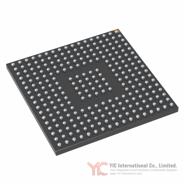
Package, pinout, and environmental characteristics of STM32H743IIK6
STM32H743IIK6 is offered in a UFBGA176+25 package (10 × 10 mm), part of a broader STM32H743xI/G portfolio that also includes other packages such as LQFP100, TFBGA100, UFBGA169, LQFP144, LQFP176, LQFP208, and TFBGA240+25.
Key package characteristics for STM32H743IIK6:
- Package / case: 176+25 UFBGA (10 × 10 mm)
- Mounting: surface‑mount, suitable for automated assembly with standard BGA handling and reflow profiles.
- Up to 168 IOs with alternate functions and interrupt capabilities, as detailed in the pinout tables and alternate function tables for each port.
Environmental and compliance:
- RoHS Status: RoHS3 compliant
- Moisture Sensitivity Level: 3 (168 hours), which defines the floor life after dry‑pack opening.
- REACH Status: REACH unaffected.
- Classification: ECCN 3A991A2 and HTSUS 8542.31.0001.
Thermal characteristics are provided in the datasheet for each package, including junction‑to‑ambient and junction‑to‑case thermal resistances, enabling accurate thermal modeling and heatsinking strategies.
12.
Electrical characteristics and operating limits of STM32H743IIK6
The STM32H743IIK6 electrical characteristics define its valid operating conditions, performance ranges, and robustness:
Voltage and current:
- Supply voltage (VDD) range: 1.62 V to 3.6 V
- Absolute maximum ratings: defined for each pin and supply domain, including maximum injection currents and voltage levels beyond which no functional guarantee is made.
- I/O characteristics: specify input thresholds, output drive capability, slew rates, and current injection limitations for each I/O port type.
Clock‑related parameters:
- External clock characteristics for HSE and LSE: define drive levels, load capacitance, and frequency ranges for external crystals or oscillators.
- Internal oscillator characteristics: accuracy, calibration ranges, and temperature profile for HSI, HSI48, CSI, and LSI.
- PLL characteristics: input/output frequency ranges, multiplication/division factors, and jitter performance.
Power consumption:
- Detailed current consumption data for Run, Sleep, Stop, Standby, and VBAT modes, including typical and maximum figures for specific use conditions (e.g., executing from ITCM, from flash with cache ON/OFF).
- Peripheral current consumption tables in Run and low‑power modes, useful for budgeting total system current under expected peripheral usage.
- Wakeup times from low‑power modes: critical when budgeting response time for interrupt‑driven applications.
Analog performance:
- ADC performance: resolution, linearity, sampling time, and conversion speed limits.
- DAC performance: settling time, linearity, and drive characteristics.
- Reference voltage buffer: output accuracy, drift, and load capabilities.
- Temperature sensor: calibration data and expected accuracy.
- OPAMP, comparator, DFSDM, DCMI, and LTDC characteristics, including timing constraints.
EMC and robustness:
- EMC characteristics and ESD absolute maximum ratings.
- I/O current injection constraints to avoid disturbance of analog operations.
Careful adherence to these characteristics allows designs based on STM32H743IIK6 to meet performance, stability, and regulatory requirements across the full operating temperature and voltage ranges.
13.
Conclusion on STM32H743IIK6 application suitability
STM32H743IIK6 brings together a 480 MHz Arm Cortex‑M7 core, a rich memory hierarchy (including 2 Mbytes flash and up to 1 Mbyte RAM), extensive analog capabilities, and a wide range of high‑speed communication interfaces. Its integrated LCD‑TFT controller, graphics accelerator, JPEG codec, DCMI, and audio interfaces support advanced HMI and multimedia use cases, while its timer set, DFSDM, OPAMP, and comparators align with motor‑control and power‑conversion applications.
The multi‑domain power architecture, voltage scaling, and low‑power modes permit fine‑tuned energy management from full‑performance operation down to microamp‑level standby and VBAT retention. Combined with security features, robust reset and clocking, and a broad set of package options, STM32H743IIK6 fits design scenarios ranging from industrial controllers and drives to networked sensors, gateways, and display‑centric embedded products.
Frequently Asked Questions (FAQ)
- Q1. What core and maximum clock frequency does STM32H743IIK6 use?
-
- A1. STM32H743IIK6 integrates a 32‑bit Arm Cortex‑M7 core running at up to 480 MHz. It includes a double‑precision FPU, DSP instructions, and 16 Kbytes each of instruction and data cache, delivering 1027 DMIPS and 2.14 DMIPS/MHz (Dhrystone 2.1).
- Q2. How much flash and RAM are available in STM32H743IIK6, and how are they organized?
-
- A2. STM32H743IIK6 provides 2 Mbytes of embedded flash memory with read‑while‑write capability. It offers up to 1 Mbyte of RAM, including 192 Kbytes of TCM RAM (64 Kbytes ITCM + 128 Kbytes DTCM) for time‑critical code and data, up to 864 Kbytes of user SRAM across various banks, and 4 Kbytes of backup SRAM in the backup domain.
- Q3. What is the operating voltage range and temperature range of STM32H743IIK6?
-
- A3. The application supply and I/Os of STM32H743IIK6 operate from 1.62 V to 3.6 V. The operating ambient temperature range is −40 °C to +85 °C (TA), suitable for industrial‑grade conditions.
- Q4. Which low‑power modes does STM32H743IIK6 support, and what functions can be retained?
-
- A4. STM32H743IIK6 supports Sleep, Stop, Standby, and VBAT modes. In Sleep mode the core is halted but peripherals can run; Stop mode keeps the regulator on and selected memories and peripherals active; in Standby mode only minimal circuitry remains powered, with RTC and backup SRAM optionally retained, yielding currents down to 2.95 μA (backup SRAM off, RTC/LSE on). VBAT mode supplies the backup domain, preserving RTC, backup SRAM, and backup registers from a backup battery.
- Q5. What analog functionalities are integrated in STM32H743IIK6?
-
- A5. STM32H743IIK6 includes 3 ADCs (up to 16‑bit resolution, 36 channels, up to 3.6 MSPS), 2 × 12‑bit DACs (1 MHz), an on‑chip temperature sensor, 2 ultra‑low‑power comparators, 2 operational amplifiers (about 7.3 MHz bandwidth), and a DFSDM block with 8 channels/4 filters for interfacing sigma‑delta modulators. It also features a voltage reference buffer and circuits for temperature and VBAT monitoring.
- Q6. Which communication interfaces are available on STM32H743IIK6?
-
- A6. STM32H743IIK6 provides up to 35 communication peripherals, including 4 I2C FM+ interfaces (SMBus/PMBus), 4 USARTs and 4 UARTs (with ISO7816, LIN, IrDA, up to 12.5 Mbit/s), 1 LPUART, 6 SPIs (3 with I2S capability), 1 additional I2S in the low‑power domain, 4 SAIs, SPDIFRX, SWPMI, MDIO slave, 2 SD/SDIO/MMC interfaces (up to 125 MHz), 2 CAN controllers (with CAN FD and time‑triggered CAN), 2 USB OTG interfaces (1 FS, 1 HS/FS with crystal‑less operation, LPM and BCD), an Ethernet MAC with dedicated DMA, and an HDMI‑CEC interface.
- Q7. Does STM32H743IIK6 support external memory expansion, and which interfaces are available?
-
- A7. Yes. STM32H743IIK6 includes a Flexible Memory Controller (FMC) supporting external SRAM, PSRAM, SDRAM/LPSDR SDRAM, NOR and NAND flash memories with up to 32‑bit data bus and synchronous operation up to 100 MHz. It also offers a dual‑mode Quad‑SPI (QUADSPI) interface running up to 133 MHz for external serial flash devices.
- Q8. What graphics and display features does STM32H743IIK6 offer?
-
- A8. STM32H743IIK6 integrates an LCD‑TFT controller supporting resolutions up to XGA, a Chrom‑ART Accelerator (DMA2D) for hardware graphics acceleration (e.g., pixel transfers, blending, color conversion), and a hardware JPEG codec for image compression and decompression. These allow the device to drive TFT displays and handle graphic GUIs with reduced CPU load.
- Q9. How can STM32H743IIK6 connect to a camera sensor?
-
- A9. STM32H743IIK6 includes an 8‑ to 14‑bit Digital Camera Interface (DCMI) with an input clock up to 80 MHz. It can capture parallel pixel data from image sensors and use DMA and external memories (e.g., SDRAM via FMC) to store and process image frames in real time.
- Q10. What timer resources does STM32H743IIK6 provide for motor control and precision timing?
-
- A10. STM32H743IIK6 has a high‑resolution timer (HRTIM1) with 2.1 ns resolution, 2 advanced‑control 16‑bit timers (TIM1, TIM8) with motor‑control features (complementary outputs, dead time, emergency stop), 2 × 32‑bit timers with IC/OC/PWM and quadrature encoder inputs (up to 240 MHz), 10 general‑purpose 16‑bit timers, 5 low‑power 16‑bit timers (LPTIM1–5), independent and window watchdogs, and a SysTick timer. This combination can generate complex PWM patterns, perform precise capture, and maintain safety supervision.
- Q11. What security and protection features are available in STM32H743IIK6?
-
- A11. STM32H743IIK6 supports readout protection (ROP) and PC‑ROP to restrict access to flash contents and execution. Active tamper functions help detect interference with secure signals. A true random number generator (RNG) with three independent oscillators provides entropy for cryptographic tasks. The embedded MPU and reset protection features support robust software isolation and recovery.
- Q12. What debug and trace options exist for STM32H743IIK6?
-
- A12. STM32H743IIK6 supports SWD and JTAG debug interfaces and includes a 4‑Kbyte embedded trace buffer. Its JTAG/SWD electrical characteristics and timing are specified to ensure reliable debug connectivity. These features facilitate non‑intrusive debugging, tracing, and performance tuning during development.
- Q13. What package is used for STM32H743IIK6, and how many I/O pins are available?
-
- A13. STM32H743IIK6 is provided in a UFBGA176+25 (10 × 10 mm) surface‑mount package. Across the STM32H743xI/G family, this package supports up to 168 I/O ports with rich alternate functions and interrupt capabilities, as described in the pin/ball definition and alternate function tables.
- Q14. Is STM32H743IIK6 compliant with RoHS and REACH requirements, and what is its MSL?
-
- A14. STM32H743IIK6 is RoHS3 compliant and REACH unaffected. Its Moisture Sensitivity Level (MSL) is 3, corresponding to a 168‑hour floor life under specified conditions after the dry‑pack is opened.
- Q15. How does STM32H743IIK6 behave during power‑up and power‑down, and what supervision features exist?
-
- A15. STM32H743IIK6 includes power‑on reset (POR), power‑down reset (PDR), programmable voltage detector (PVD), and brown‑out reset (BOR) to control startup and shutdown behavior. The embedded reset and power control block has defined operating conditions and timing for power‑up and power‑down. These features help ensure that the device only leaves reset when supply levels are within specified ranges and allow configurable responses to supply dips.
- Q16. How is device uniqueness handled in STM32H743IIK6?
-
- A16. STM32H743IIK6 contains a 96‑bit unique device ID programmed during manufacturing. This ID can be used by firmware for device serialization, licensing, or secure provisioning and pairing schemes.