Product overview of STM32H743XIH6 STM32H7 microcontroller
STM32H743XIH6 is a high‑performance 32‑bit microcontroller in the STM32H7 family from STMicroelectronics. It integrates an Arm Cortex‑M7 single core running up to 480 MHz with double‑precision floating‑point unit (FPU), DSP extensions, and L1 caches, delivering up to 1027 DMIPS and 2.14 DMIPS/MHz (Dhrystone 2.1).
The STM32H743XIH6 STM32H7 device combines up to 2 MB of embedded Flash, up to 1 MB of RAM, a rich set of communication interfaces, advanced timers, extensive analog peripherals, and dedicated accelerators for graphics and multimedia. It is offered in a 240+25‑ball TFBGA package (14 × 14 mm) with up to 168 general‑purpose I/Os and supports an operating temperature range of −40 °C to 85 °C.
Key feature highlights of STM32H743XIH6 STM32H7 include:
- 32‑bit Arm Cortex‑M7 core at 480 MHz with double‑precision FPU, instruction and data caches, MPU, and DSP instructions.
- Up to 2 MB Flash with read‑while‑write, and up to 1 MB RAM including tightly coupled ITCM/DTCM.
- Supply voltage range 1.62 V to 3.6 V, integrated LDO regulator, USB‑dedicated 3.3 V regulator, and multiple low‑power modes.
- Three ADCs up to 16‑bit resolution, two DACs, comparators, op‑amps, temperature sensor, and DFSDM.
- LCD‑TFT controller, Chrom‑ART (DMA2D) accelerator, hardware JPEG codec, and DCMI camera interface.
- Rich connectivity: multiple I2C, USART/UART/LPUART, SPI/I2S, SAI, SPDIFRX, SWPMI, SDMMC, FDCAN with CAN FD and TT‑CAN, USB OTG HS/FS, Ethernet MAC with DMA, HDMI‑CEC.
- Hardware cryptographic‑related features such as true random number generator (RNG) and security mechanisms like readout protection (ROP), PC‑ROP, and active tamper.
- RoHS3 compliant, REACH unaffected, MSL3 (168 hours) moisture sensitivity level.
STM32H743XIH6 STM32H7 provides a platform suited to high‑performance control, advanced human‑machine interfaces, data acquisition, and connected embedded nodes where processing throughput, integrated memory, and peripheral richness drive device choice.
2.
Core architecture and processing capabilities of STM32H743XIH6 STM32H7
At the heart of STM32H743XIH6 STM32H7 lies a 32‑bit Arm Cortex‑M7 core with:
- Maximum clock frequency of 480 MHz.
- Double‑precision FPU, supporting complex numeric algorithms directly on the MCU.
- L1 cache: 16 Kbytes instruction cache and 16 Kbytes data cache.
- DSP instruction set, enabling efficient digital signal processing functions.
- Memory Protection Unit (MPU) to partition memory regions for robustness and software separation.
The core’s performance, expressed as up to 1027 DMIPS, allows STM32H743XIH6 STM32H7 to handle compute‑intensive tasks such as motor control algorithms, digital filtering, real‑time data analytics, and complex GUI rendering without offloading to external processors.
Real‑world example: In an industrial motor control application, the STM32H743XIH6 STM32H7 Cortex‑M7 core can simultaneously execute field‑oriented control, sensor fusion from multiple ADC channels, and communication protocol stacks. The FPU and DSP instructions reduce cycle counts for trigonometric, filtering, and control computations, enabling higher PWM frequencies and finer torque control while maintaining communication responsiveness.
3.
Memory subsystem and data throughput in STM32H743XIH6 STM32H7
The memory structure of STM32H743XIH6 STM32H7 is aligned with high‑speed execution requirements and flexible data storage.
Embedded Flash memory in STM32H743XIH6 STM32H7:
- Up to 2 Mbytes of embedded Flash (2M × 8) for program storage.
- Read‑while‑write capability, allowing firmware to update sections of Flash while executing code from another area.
- Memory mapping optimized for fast code execution, particularly when combined with caches and ITCM.
Embedded RAM in STM32H743XIH6 STM32H7 is segmented:
- Up to 192 Kbytes of TCM RAM:
- 64 Kbytes ITCM RAM for time‑critical instruction execution.
- 128 Kbytes DTCM RAM for time‑critical data.
- Up to 864 Kbytes of user SRAM, accessible via AXI/AHB buses for general data storage, buffers, and stack/heap.
- 4 Kbytes of SRAM in the Backup domain, retained in VBAT mode for low‑power retention of key parameters.
External memory expansion is supported by:
- Flexible Memory Controller (FMC) in STM32H743XIH6 STM32H7 with up to 32‑bit data bus for SRAM, PSRAM, NOR/NAND Flash, and SDRAM/LPSDR SDRAM, running up to 100 MHz in synchronous mode.
- Dual‑mode Quad‑SPI (QUADSPI) memory interface in STM32H743XIH6 STM32H7, running up to 133 MHz, enabling external serial NOR Flash or Hyper‑type memories for code and data.
Memory access is orchestrated via a high‑bandwidth interconnect:
- 3 bus matrices (1 AXI and 2 AHB) in STM32H743XIH6 STM32H7.
- Multiple AHB and AXI‑AHB bridges to connect masters (CPU, DMA, MDMA) and slaves (memories, peripherals).
- Four DMA controllers including:
- One high‑speed master DMA (MDMA) with linked‑list support.
- Two dual‑port DMAs with FIFO.
- One basic DMA with configurable request router.
Real‑world example: A data‑logging node using STM32H743XIH6 STM32H7 can sample multiple ADC channels at high speed, store data in on‑chip SRAM, and use MDMA to stream data to external SDRAM or Quad‑SPI Flash, while the CPU runs analysis and communication stacks. The bus matrices and DMAs reduce contention and increase sustained throughput.
4.
Power supply, domains and low‑power modes in STM32H743XIH6 STM32H7
STM32H743XIH6 STM32H7 offers a flexible power architecture designed to balance performance with consumption.
Supply and regulators in STM32H743XIH6 STM32H7:
- Application supply and I/O voltage: 1.62 V to 3.6 V.
- Embedded LDO regulator with configurable and scalable output to supply digital circuitry.
- Dedicated 3.3 V USB power regulator for internal USB PHYs.
- Embedded backup regulator (~0.9 V) for backup domain and VBAT operation.
- Internal voltage reference for analog peripherals (VREF+).
Power domains in STM32H743XIH6 STM32H7:
- Three power domains:
- D1: high‑performance capabilities domain (CPU, high‑speed interfaces).
- D2: communication peripherals and timers.
- D3: reset/clock control and power management, plus backup domain.
- Domains can be individually clock‑gated or switched off, allowing fine‑grained power control.
Low‑power modes in STM32H743XIH6 STM32H7:
- Sleep mode: core clock stopped, peripherals running; quick wake‑up.
- Stop mode: regulator on, clocks gated, sections of domains off; balancing retention with reduced current.
- Standby mode: lowest system state with context lost except backup domain; typical current around 2.95 µA (Backup SRAM OFF, RTC/LSE ON).
- VBAT mode: backup domain powered from VBAT pin with battery operation and optional battery charging.
Voltage scaling:
- Six configurable voltage scaling ranges in Run and Stop modes for STM32H743XIH6 STM32H7 allow tuning of power vs. maximum frequency.
Real‑world example: A connected metering node based on STM32H743XIH6 STM32H7 can periodically wake from Stop mode to sample sensors and send data over Ethernet or CAN, then return to low‑power mode. The separate domains ensure that only the logic strictly needed during idle periods remains powered.
5.
Clock, reset, and bus matrix design of STM32H743XIH6 STM32H7
Clock sources in STM32H743XIH6 STM32H7:
- Internal oscillators:
- 64 MHz HSI.
- 48 MHz HSI48 (suited for USB and RNG).
- 4 MHz CSI.
- 32 kHz LSI.
- External oscillators:
- 4–48 MHz HSE for main high‑speed clock.
- 32.768 kHz LSE for RTC and calendar accuracy.
Phase‑locked loops (PLLs) in STM32H743XIH6 STM32H7:
- Three PLLs:
- One main PLL for the system clock.
- Two additional PLLs for kernel clocks (e.g., USB, SAI, LTDC).
- Fractional mode support for fine frequency tuning.
Reset and clock control (RCC) in STM32H743XIH6 STM32H7:
- Centralized clock tree configuration per domain.
- Multiple system reset sources: power‑on reset (POR), power‑down reset (PDR), brown‑out reset (BOR), software reset, watchdog resets.
- Embedded power supply supervisor for monitoring VDD and managing safe start‑up and brown‑out conditions.
Interconnect matrix in STM32H743XIH6 STM32H7:
- 3 bus matrices (1 AXI, 2 AHB) with multiple masters and slaves.
- Five AHB2‑APB bridges and two AXI‑to‑AHB bridges.
- Architecture supports concurrent high‑bandwidth transactions between core, DMAs, and peripherals, minimizing latency for real‑time tasks.
Real‑world example: In a display‑centric product using STM32H743XIH6 STM32H7, LTDC and DMA2D can fetch graphics from internal or external SDRAM via AXI while the CPU accesses TCM RAM for real‑time control; separate matrices and bridges help sustain both without visible UI lag.
6.
Analog and mixed‑signal resources in STM32H743XIH6 STM32H7
STM32H743XIH6 STM32H7 integrates a broad analog feature set for measurement, conditioning, and conversion.
ADC subsystem in STM32H743XIH6 STM32H7:
- Three ADCs with up to 16‑bit maximum resolution.
- Up to 36 external channels.
- Sampling rate up to 3.6 MSPS.
- Internal temperature sensor accessible via ADC.
DAC subsystem in STM32H743XIH6 STM32H7:
- Two 12‑bit digital‑to‑analog converters.
- Conversion rate up to 1 MHz, suitable for waveform generation, offset generation, or analog control signals.
Comparators and op‑amps in STM32H743XIH6 STM32H7:
- Two ultra‑low‑power comparators for threshold detection and window comparisons with minimal power.
- Two operational amplifiers with 7.3 MHz bandwidth, allowing configurable amplification for sensor signals and conditioning for ADC inputs.
DFSDM in STM32H743XIH6 STM32H7:
- Digital filter for sigma‑delta modulators (DFSDM) with up to 8 input channels and 4 digital filters.
- Intended for interfacing with external sigma‑delta modulators, enabling high‑precision current sensing or audio‑grade measurements.
Additional analog features in STM32H743XIH6 STM32H7:
- Embedded voltage reference buffer.
- Temperature and VBAT monitoring capabilities.
- Voltage booster for analog switch, supporting proper analog routing over a wider supply range.
Real‑world example: In a power monitoring unit, STM32H743XIH6 STM32H7 can use ADCs to measure voltages, DFSDM for accurate current sensing through external shunt modulators, op‑amps for signal conditioning, and DACs to provide reference signals for calibration routines.
7.
Timer resources and motor/control timing in STM32H743XIH6 STM32H7
Timer resources in STM32H743XIH6 STM32H7 cover high‑resolution control, general timing, and low‑power timekeeping:
High‑resolution timer (HRTIM1) in STM32H743XIH6 STM32H7:
- Maximum resolution around 2.1 ns.
- Suitable for fine‑step PWM in digital power conversion and high‑frequency motor control.
Advanced‑control timers (TIM1, TIM8) in STM32H743XIH6 STM32H7:
- 16‑bit timers running up to 240 MHz.
- Up to four channels with input capture/output compare/PWM.
- Support for complementary outputs and dead‑time insertion for motor control and power stages.
General‑purpose timers in STM32H743XIH6 STM32H7:
- Ten 16‑bit general‑purpose timers (up to 240 MHz).
- Two 32‑bit timers with up to four input capture/output compare/PWM channels; can function as quadrature encoders and high‑frequency counters.
Low‑power timers in STM32H743XIH6 STM32H7:
- Five low‑power timers (LPTIM1–LPTIM5) operating up to 240 MHz, designed to remain functional in low‑power modes for wake‑up and periodic tasks.
Basic timers, watchdogs and system tick in STM32H743XIH6 STM32H7:
- Basic timers TIM6 and TIM7 for simple time‑base generation.
- Independent watchdog and window watchdog for system monitoring and recovery from software anomalies.
- SysTick timer for OS tick and basic timekeeping.
Real‑world example: A multi‑axis motor driver using STM32H743XIH6 STM32H7 may use HRTIM1 for high‑frequency PWM to control a power stage, TIM1/TIM8 for phase‑shifted PWMs with dead‑time, and 32‑bit timers as encoder interfaces, while watchdogs supervise runtime and LPTIMs handle wake‑up scheduling in reduced‑power states.
8.
Communication interfaces and connectivity options in STM32H743XIH6 STM32H7
STM32H743XIH6 STM32H7 integrates a wide range of communication interfaces, enabling direct connection to fieldbuses, storage devices, and high‑speed links.
Serial interfaces in STM32H743XIH6 STM32H7:
- Four I2C Fast‑mode Plus interfaces with SMBus/PMBus support.
- Four USARTs and four UARTs supporting ISO7816 smartcard, LIN, IrDA, and up to 12.5 Mbit/s data rates.
- One low‑power UART (LPUART) optimized for low‑energy serial communication.
SPI/I2S and audio‑related interfaces in STM32H743XIH6 STM32H7:
- Six SPI interfaces, three with multiplexed full‑duplex I2S audio capability (up to 150 MHz).
- Four SAI (Serial Audio Interface) blocks for flexible audio formats and multichannel audio.
- One SPDIFRX receiver for digital audio input.
- Clocking options via internal audio PLL or external clock.
Additional digital communication in STM32H743XIH6 STM32H7:
- SWPMI single‑wire protocol master interface.
- MDIO slave interface for Ethernet PHY management.
- Two SD/SDIO/MMC interfaces up to 125 MHz for memory cards.
Network and fieldbus in STM32H743XIH6 STM32H7:
- Two FDCAN controllers, supporting CAN FD and time‑triggered CAN (TT‑CAN) for deterministic networked control.
- Ethernet MAC with dedicated DMA controller, enabling high‑throughput network communication.
USB and consumer electronics control in STM32H743XIH6 STM32H7:
- Two USB OTG interfaces: one FS and one HS/FS.
- Support for crystal‑less USB operation, Link Power Management (LPM), and Battery Charging Detection (BCD).
- HDMI‑CEC interface for consumer electronics control over HDMI.
Real‑world example: A gateway design based on STM32H743XIH6 STM32H7 can bridge FDCAN networks, Ethernet, and USB, while logging to SD card and sharing audio data via SAI; integrated DMAs and dedicated MAC DMA sustain channel throughput without saturating the CPU.
9.
Graphics, imaging, and multimedia acceleration in STM32H743XIH6 STM32H7
STM32H743XIH6 STM32H7 includes hardware to support advanced user interfaces and multimedia streaming.
Graphics acceleration in STM32H743XIH6 STM32H7:
- Chrom‑ART Accelerator (DMA2D) offloads 2D graphics operations such as fills, pixel format conversion, and image blending. This reduces CPU load during GUI rendering.
- LCD‑TFT controller (LTDC) capable of driving displays up to XGA resolution, supporting layered framebuffers.
Imaging and compression in STM32H743XIH6 STM32H7:
- Digital camera interface (DCMI) supporting 8‑ to 14‑bit parallel cameras up to 80 MHz pixel clock.
- Hardware JPEG Codec to compress and decompress image streams, reducing storage and bandwidth requirements.
Real‑world example: A touchscreen HMI powered by STM32H743XIH6 STM32H7 can use LTDC to drive a TFT panel, DMA2D to composite UI elements in real time, DCMI to capture camera frames, and the JPEG codec to compress snapshots for storage or transmission. This combination enables responsive UIs and camera features without needing a dedicated application processor.
10.
Security, debug, and system management features of STM32H743XIH6 STM32H7
Security‑related features in STM32H743XIH6 STM32H7:
- Readout protection (ROP) and PC‑ROP allow configuring different levels of Flash memory access protection, helping guard firmware from unauthorized readout.
- Active tamper capability integrated with backup domain to detect attempts to manipulate secure state.
- True random number generator (RNG) with three internal oscillators feeding entropy, supporting cryptographic protocols and secure key generation.
- 96‑bit unique device ID for device identification and provisioning schemes.
Debug infrastructure in STM32H743XIH6 STM32H7:
- SWD and JTAG interfaces for programming, debugging, and boundary scan.
- Embedded 4‑Kbyte trace buffer, supporting advanced trace features for performance analysis and fault diagnostics.
System management in STM32H743XIH6 STM32H7:
- Nested vectored interrupt controller (NVIC) for prioritizing and managing interrupts with low latency.
- Extended interrupt and event controller (EXTI) for configuring external and internal events as triggers.
- Cyclic redundancy check (CRC) calculation unit to accelerate frame integrity checks and data verification.
- RTC with sub‑second precision, calendar hardware, backup registers, and backup SRAM.
Real‑world example: A secure data logger using STM32H743XIH6 STM32H7 can generate cryptographic nonces with RNG, store keys in protected Flash regions, monitor tamper inputs via backup domain, and record timestamps using the RTC while protecting firmware from extraction using ROP settings.
11.
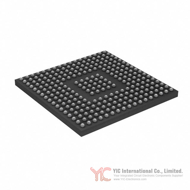
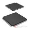
Package, pinout and environmental characteristics of STM32H743XIH6 STM32H7
Packaging for STM32H743XIH6 STM32H7:
- STM32H743XIH6 is packaged in a 240+25‑ball TFBGA (14 × 14 mm).
- Up to 168 general‑purpose input/output ports with interrupt capability.
- I/Os support multiple alternate functions allowing routing of interfaces such as Ethernet, SDMMC, FMC, LTDC, and others.
Environmental and compliance parameters for STM32H743XIH6 STM32H7:
- Operating temperature range: −40 °C to 85 °C (TA).
- RoHS3 compliant and REACH unaffected.
- Moisture Sensitivity Level (MSL): 3 (168 hours floor life).
The large pin‑count package of STM32H743XIH6 STM32H7 supports wide bus interfaces and parallel display or camera buses, making it suitable where extensive external connectivity and memory expansion are needed.
12.
Electrical performance and operating conditions of STM32H743XIH6 STM32H7
Operating conditions for STM32H743XIH6 STM32H7:
- Supply voltage range: 1.62 V to 3.6 V across application supply and I/Os.
- Detailed operating conditions at power‑up and power‑down, including constraints on ramp times and reset behavior.
- External VCAP capacitor requirements for internal regulator stability.
Current consumption characteristics in STM32H743XIH6 STM32H7:
- Current consumption specified for Run mode under various conditions:
- Code running from ITCM.
- Code running from Flash with cache ON/OFF.
- Typical and maximum currents defined for Sleep, Stop, Standby, and VBAT modes, allowing estimation of energy budget.
- Peripheral‑specific consumption data in Run, Stop, Standby and VBAT modes.
Clock source characteristics for STM32H743XIH6 STM32H7:
- HSE external clock and crystal parameters (4–48 MHz) with recommended loading capacitors and drive.
- LSE and LSI timing and accuracy constraints.
- Internal oscillator (HSI, HSI48, CSI) performance and calibration data.
- PLL characteristics for frequency planning.
I/O and EMC characteristics of STM32H743XIH6 STM32H7:
- I/O current injection limits and port drive characteristics (input thresholds, output current, rise/fall times).
- NRST pin characteristics for reliable reset control.
- EMC performance and electrical sensitivity ratings, including ESD and latch‑up limits.
Analog performance characteristics in STM32H743XIH6 STM32H7:
- ADC: resolution, INL/DNL, sampling time, input impedance, and timing for different modes.
- DAC: output drive, settling time, and noise characteristics.
- Reference buffer, temperature sensor, comparators and op‑amps electrical parameters.
- DFSDM, DCMI and LTDC timing constraints for reliable high‑speed operation.
These parameters allow STM32H743XIH6 STM32H7 to be dimensioned correctly within power, thermal, and signal integrity budgets for a given design.
13.
Application scenarios and selection considerations for STM32H743XIH6 STM32H7
Based on its feature set, STM32H743XIH6 STM32H7 fits application scenarios that demand high compute density, extensive connectivity, and integrated graphics/analog.
Typical usage patterns for STM32H743XIH6 STM32H7:
- High‑performance industrial control: multi‑axis motor drives, digital power, and plant automation, leveraging HRTIM, advanced timers, FDCAN, and high‑precision ADC/DFSDM.
- Human‑machine interfaces: graphical panels and control consoles using LTDC, Chrom‑ART (DMA2D), JPEG, and audio interfaces (SAI, I2S).
- Connected data concentrators: Ethernet, USB OTG, SDMMC, and multiple UART/I2C/SPI channels for protocol bridging and data logging.
- Measurement and instrumentation: high‑resolution ADCs, DACs, op‑amps, comparators, and RTC for precision acquisition and timestamping.
Selection drivers for STM32H743XIH6 STM32H7 include:
- Need for 480 MHz single‑core performance with FPU and DSP.
- Requirements for large embedded memory (2 MB Flash, up to 1 MB RAM) and external memory interfaces (FMC, Quad‑SPI) for code/data expansion.
- Requirement to integrate camera, display, and compression without an external application processor.
- Networking needs involving Ethernet + FDCAN + USB, with hardware DMA support.
- Requirement to consolidate analog acquisition, graphics, and control on a single microcontroller.
Real‑world example: A combined control and visualization unit for an industrial machine can be built around STM32H743XIH6 STM32H7, combining motor control, safety monitoring, Ethernet connectivity, local logging to SD card, and a TFT‑based GUI, reducing component count compared to separate control and HMI processors.
14.
Conclusion on STM32H743XIH6 STM32H7 capabilities
STM32H743XIH6 STM32H7 integrates a 480 MHz Cortex‑M7 core with up to 2 MB Flash and up to 1 MB RAM, coupled with advanced analog, timers, connectivity, and dedicated graphics/multimedia accelerators in a high‑pin‑count TFBGA package. Its multi‑domain power architecture, extensive low‑power modes, and rich clocking options enable deployment in performance‑oriented systems as well as energy‑sensitive equipment.
The combination of FMC, Quad‑SPI, LTDC, DMA2D, JPEG, DCMI, FDCAN, Ethernet, USB OTG HS/FS, high‑resolution timers, and 16‑bit ADCs positions STM32H743XIH6 STM32H7 as a single‑chip platform for applications that merge real‑time control, connectivity, and advanced user interfaces. Detailed electrical, timing, and environmental specifications support robust design across industrial temperature ranges and varied operating conditions.
15.
Frequently Asked Questions (FAQ)
- Q1. What is the core architecture and performance level of STM32H743XIH6 STM32H7?
-
- A1. STM32H743XIH6 STM32H7 is based on a 32‑bit Arm Cortex‑M7 single core running up to 480 MHz. It integrates a double‑precision FPU, DSP instructions, and 16 Kbytes each of instruction and data cache. The device delivers up to 1027 DMIPS, which allows it to handle compute‑intensive control, signal processing, and GUI tasks without external processors.
- Q2. How much Flash and RAM does STM32H743XIH6 STM32H7 provide, and can it be expanded?
-
- A2. STM32H743XIH6 STM32H7 integrates up to 2 MB of embedded Flash memory with read‑while‑write capability and up to 1 MB of RAM, including 192 Kbytes of TCM RAM (64 Kbytes ITCM + 128 Kbytes DTCM), up to 864 Kbytes of user SRAM, and 4 Kbytes of backup SRAM. External memory expansion is possible through FMC (supporting SRAM, PSRAM, SDRAM/LPSDR SDRAM, NOR/NAND Flash with up to 32‑bit bus at up to 100 MHz synchronous) and through the dual‑mode Quad‑SPI interface running up to 133 MHz.
- Q3. What supply voltage and temperature range does STM32H743XIH6 STM32H7 support?
-
- A3. The application supply and I/O voltage range for STM32H743XIH6 STM32H7 is 1.62 V to 3.6 V. The operating ambient temperature range is −40 °C to 85 °C. The device integrates an LDO regulator for core supply, a dedicated 3.3 V regulator for USB PHYs, and a backup regulator for VBAT and backup domain operation.
- Q4. Which low‑power modes are available in STM32H743XIH6 STM32H7, and what kind of currents are expected?
-
- A4. STM32H743XIH6 STM32H7 supports Sleep, Stop, Standby, and VBAT modes. In Sleep mode, the core clock is stopped while most peripherals can remain active. Stop mode keeps the regulator on but gates most clocks, allowing state retention with reduced consumption. Standby mode powers down most of the device, retaining only the backup domain; typical current in Standby is about 2.95 µA with Backup SRAM off and RTC/LSE on. VBAT mode powers only the backup domain (RTC, backup registers, backup SRAM) through the VBAT pin for battery‑backed retention.
- Q5. What analog interfaces does STM32H743XIH6 STM32H7 offer for measurement and signal conditioning?
-
- A5. STM32H743XIH6 STM32H7 integrates three ADCs with up to 16‑bit resolution, up to 36 channels and up to 3.6 MSPS, suitable for precision and high‑speed sampling. It has two 12‑bit DACs with 1 MHz conversion rate, two ultra‑low‑power comparators, two operational amplifiers with 7.3 MHz bandwidth, a digital filter for sigma‑delta modulators (DFSDM) with up to 8 inputs and 4 filters, a temperature sensor, and a voltage reference buffer. This set allows direct connection to many sensors and analog front‑ends.
- Q6. How does STM32H743XIH6 STM32H7 support motor control and high‑resolution timing?
-
- A6. STM32H743XIH6 STM32H7 includes a high‑resolution timer (HRTIM1) with a resolution down to around 2.1 ns, suited for digital power and high‑frequency PWM. It also offers two advanced‑control timers (TIM1, TIM8) with complementary outputs and dead‑time insertion, ten 16‑bit general‑purpose timers, two 32‑bit timers, five low‑power timers, and basic timers. Combined with high‑speed ADCs and DFSDM, these timers enable sophisticated motor‑control and power‑conversion schemes.
- Q7. Which communication interfaces are integrated in STM32H743XIH6 STM32H7 for connectivity?
-
- A7. STM32H743XIH6 STM32H7 provides four I2C Fast‑mode Plus interfaces (with SMBus/PMBus), four USARTs and four UARTs (supporting ISO7816, LIN, IrDA), one low‑power UART, six SPI (three with I2S support), four SAI blocks, one SPDIFRX, one SWPMI, an MDIO slave, two SD/SDIO/MMC interfaces up to 125 MHz, two FDCAN controllers supporting CAN FD and TT‑CAN, an Ethernet MAC with dedicated DMA, and two USB OTG interfaces (one FS, one HS/FS) with crystal‑less operation, LPM, and BCD. There is also an HDMI‑CEC interface for consumer electronics control.
- Q8. Does STM32H743XIH6 STM32H7 support LCD displays and camera modules directly?
-
- A8. Yes. STM32H743XIH6 STM32H7 includes an LCD‑TFT controller (LTDC) capable of driving displays up to XGA resolution, along with a Chrom‑ART (DMA2D) accelerator for 2D graphics operations. It also features an 8‑ to 14‑bit DCMI interface with up to 80 MHz pixel clock for connection to parallel camera sensors. The integrated JPEG codec can compress and decompress image data in hardware.
- Q9. What hardware accelerators does STM32H743XIH6 STM32H7 include for offloading the CPU?
-
- A9. Beyond the FPU and DSP instruction set in the Cortex‑M7 core, STM32H743XIH6 STM32H7 integrates:
- Chrom‑ART Accelerator (DMA2D) for graphics.
- Hardware JPEG codec.
- Multiple DMA engines, including one high‑speed MDMA with linked‑list support, two dual‑port DMAs with FIFO, and one basic DMA.
- Dedicated DMA for Ethernet MAC.
These accelerators reduce CPU load for graphics, data movement, compression, and communication. - Q10. What security‑related features are available in STM32H743XIH6 STM32H7?
-
- A10. STM32H743XIH6 STM32H7 offers readout protection (ROP) and PC‑ROP to restrict access to Flash contents, active tamper detection in the backup domain, and a true random number generator (RNG) based on three internal oscillators. The device also includes a 96‑bit unique ID for device identification. These features support securing firmware, protecting keys, and generating randomness for secure protocols.
- Q11. How does STM32H743XIH6 STM32H7 handle backup and real‑time clock functionality?
-
- A11. STM32H743XIH6 STM32H7 has an RTC with sub‑second accuracy, hardware calendar, and dedicated backup registers. It provides 4 Kbytes of backup SRAM and a VBAT supply pin to keep the backup domain powered from a battery when main VDD is off. The RTC can run from LSE or other low‑frequency sources, and backup registers/SRAM retain system parameters and time across power cycles and Standby.
- Q12. What is the package type and I/O capability of STM32H743XIH6 STM32H7?
-
- A12. STM32H743XIH6 STM32H7 is offered in a 240+25‑ball TFBGA package (14 × 14 mm). It exposes up to 168 general‑purpose I/O ports, each capable of hosting multiple alternate functions, including high‑speed interfaces like FMC, SDMMC, Ethernet, LTDC, DCMI, and others. The package and pin mapping are designed to support dense external connections and wide external buses.
- Q13. How does STM32H743XIH6 STM32H7 support USB applications?
-
- A13. The device integrates two USB OTG controllers: one full‑speed (FS) and one high‑speed/full‑speed (HS/FS). It supports crystal‑less USB operation using internal oscillators, and features Link Power Management (LPM) and Battery Charging Detection (BCD). A dedicated 3.3 V regulator supplies the internal USB PHYs. These capabilities enable STM32H743XIH6 STM32H7 to function as USB device, host, or OTG in various configurations.
- Q14. What identification and trace features does STM32H743XIH6 STM32H7 provide for development and production?
-
- A14. STM32H743XIH6 STM32H7 includes a 96‑bit unique device ID that can be used in production to distinguish units and manage provisioning. For development and diagnostics, it offers SWD and JTAG debug interfaces plus a 4‑Kbyte embedded trace buffer. These facilities allow in‑circuit debugging, trace capture, and profiling during firmware development and system validation.
- Q15. How should external capacitors and power‑up conditions be considered when designing with STM32H743XIH6 STM32H7?
-
- A15. The datasheet for STM32H743XIH6 STM32H7 specifies operating conditions for the VCAP pins associated with the internal regulator, including recommended capacitance values and ESR to ensure regulator stability. It also defines constraints on power‑up and power‑down sequences, including minimum ramp times and conditions for reset release. Adhering to these ensures proper startup, reliable BOR/POR operation, and stable internal voltage regulation.
- Q16. What are the compliance and environmental robustness characteristics of STM32H743XIH6 STM32H7?
-
- A16. STM32H743XIH6 STM32H7 is RoHS3 compliant and REACH unaffected. It has a Moisture Sensitivity Level (MSL) of 3 with a 168‑hour floor life and is rated for operation from −40 °C to 85 °C. Electrical characteristics include ESD and latch‑up robustness figures, as well as EMC performance data, which guide layout, protection, and handling practices in production environments.