STM32H743BIT6 product overview
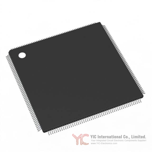
The STM32H743BIT6 is a 32-bit microcontroller from STMicroelectronics in the STM32H7 series, specifically within the STM32H743xI/G family. It integrates a single-core Arm Cortex-M7 CPU running at up to 480 MHz, with up to 2 MB of embedded flash memory and up to 1 MB of RAM. In the STM32H743BIT6 variant, the package is 208-LQFP with dimensions of 28 × 28 mm, and the device is specified for surface-mount assembly.
From a system perspective, the STM32H743BIT6 combines high CPU throughput, a layered memory architecture, broad communication coverage, analog integration, display support, audio interfaces, camera input capability, hardware JPEG processing, and a graphics accelerator. The datasheet positions the STM32H742xI/G and STM32H743xI/G devices as microcontrollers with up to 46 communication and analog interfaces, which reflects the breadth of on-chip resources available for designs that consolidate control, connectivity, signal acquisition, and user-interface functions into a single MCU.
The supply range is 1.62 V to 3.6 V for application supply and I/Os. The device includes reset and power supervision features such as POR, PDR, PVD, and BOR, and it supports several low-power modes including Sleep, Stop, Standby, and VBAT. For long-term timekeeping and backup-domain retention use cases, it also provides backup SRAM and RTC-related resources.
At the feature level, the STM32H743BIT6 includes up to 168 I/O ports, multiple DMA engines, a flexible external memory controller, a Quad-SPI interface running up to 133 MHz, up to 22 timers and watchdogs, three ADCs with 16-bit maximum resolution, two 12-bit DACs, ultra-low-power comparators, operational amplifiers, digital filters for sigma-delta modulators, Ethernet, USB OTG, FDCAN, SDMMC, SPI/I2S, SAI, USART/UART/LPUART, I2C, and display-oriented blocks such as LTDC and Chrom-ART Accelerator. This mix makes the device suitable for designs that need both computational capability and extensive peripheral integration.
STM32H743BIT6 architecture and processing performance
At the center of the STM32H743BIT6 is an Arm Cortex-M7 core with double-precision floating-point unit, DSP instructions, memory protection unit, and L1 cache consisting of 16 KB instruction cache and 16 KB data cache. STMicroelectronics specifies performance up to 1027 DMIPS and 2.14 DMIPS/MHz based on Dhrystone 2.1, with operating frequency up to 480 MHz.
This processing profile shapes how the STM32H743BIT6 can be used. The Cortex-M7 core is designed to handle control algorithms, signal processing, communication stacks, and graphics-related workloads with lower software overhead than a simpler MCU core. The inclusion of DSP instructions supports mathematically intensive tasks such as filtering, motor-control calculations, and digital signal analysis, while the double-precision FPU expands suitability for applications where floating-point accuracy or software portability is desired.
The MCU is partitioned into three power and clock domains:
D1 for high-performance capabilities,
D2 for communication peripherals and timers,
D3 for reset, clock control, and power management.
This domain structure is useful when balancing throughput and power consumption, because parts of the device can be clock-gated or switched off independently. In practice, that means a design can keep a subset of interfaces or supervisory functions active while reducing activity in higher-performance logic blocks.
The interconnect architecture also supports the performance goal. The STM32H743BIT6 integrates three bus matrices, one AXI and two AHB, along with multiple bridges between AHB, APB, and AXI segments. This arrangement helps separate CPU, DMA, memory, and peripheral traffic so that data movement and peripheral servicing do not rely entirely on the CPU path.
A practical example is an embedded HMI node that captures image data, updates a display, and exchanges control messages over Ethernet or CAN. In that case, the Cortex-M7 handles application logic while DMA and specialized engines move display or image data in parallel, reducing contention compared with a simpler shared-bus arrangement.
STM32H743BIT6 memory organization and data handling
The STM32H743BIT6 provides up to 2 MB of flash memory with read-while-write support and up to 1 MB of RAM. STMicroelectronics details the RAM structure as 192 KB of TCM RAM, including 64 KB of ITCM RAM and 128 KB of DTCM RAM for time-critical routines, up to 864 KB of user SRAM, and 4 KB of SRAM in the backup domain.
This memory hierarchy is one of the defining characteristics of the STM32H743BIT6. It is not simply a large flash-plus-RAM arrangement; it is organized so that software can place different code and data types where they fit best. Time-sensitive routines can be stored in TCM RAM, while larger buffers, communication payloads, and general application data can reside in user SRAM. The presence of read-while-write support in embedded flash also helps in applications that need firmware updates or flash operations without fully halting code execution in all scenarios.
For external expansion, the STM32H743BIT6 includes a Flexible Memory Controller with up to a 32-bit data bus supporting SRAM, PSRAM, SDRAM/LPSDR SDRAM, and NOR/NAND flash, with memory clocked up to 100 MHz in synchronous mode. It also includes a dual-mode Quad-SPI memory interface running up to 133 MHz.
These interfaces broaden system architecture choices. A design that needs frame buffers, large data logs, external code storage, or expandable memory can pair the MCU with external memory devices. For instance, LTDC-based display applications may place larger frame data in external SDRAM through FMC, while QSPI flash can hold fonts, graphics assets, or application images. Because the MCU already integrates graphics acceleration and a JPEG codec, the external memory interfaces complement those blocks in display-oriented systems.
The device also includes a CRC calculation unit, which supports integrity checking for transferred or stored data. In systems that move firmware images, configuration blocks, or communication packets, CRC can reduce CPU involvement in data-verification routines.
STM32H743BIT6 power, reset, clocking, and low-power operation
The STM32H743BIT6 operates from a 1.62 V to 3.6 V application supply and I/O range. It provides POR, PDR, PVD, and BOR functions for supply supervision. STMicroelectronics also specifies a dedicated USB power embedding a 3.3 V internal regulator to supply the internal PHYs, an embedded LDO with configurable scalable output to supply digital circuitry, and a backup regulator around 0.9 V.
Voltage scaling is available in Run and Stop modes across six configurable ranges. This allows the system to trade maximum performance for lower power depending on operating state. The device supports Sleep, Stop, Standby, and VBAT modes, and the datasheet lists standby current down to 2.95 µA with Backup SRAM off and RTC/LSE on. There is also VBAT battery operating mode with charging support.
The three-domain architecture appears again in the power strategy. Since D1, D2, and D3 can be independently clock-gated or switched off, the STM32H743BIT6 can be adapted to use cases where some resources must remain active while others are suspended. A communication gateway, for example, may keep RTC, wakeup logic, and selected communication functions available while reducing the rest of the system to a lower-power state between bursts of traffic.
Clock management includes internal oscillators:
64 MHz HSI,
48 MHz HSI48,
4 MHz CSI,
32 kHz LSI.
External oscillators include:
4–48 MHz HSE,
32.768 kHz LSE.
The device further integrates three PLLs, one for system clock and two for kernel clocks, with fractional mode. This clock tree gives the STM32H743BIT6 flexibility when multiple high-speed peripherals need different clock conditions. USB, audio, timers, CPU core, and communication interfaces can be tuned more independently than on MCUs with a simpler clock scheme.
Reset handling is part of the same system-management layer. The datasheet includes system reset sources and reset/power-control block characteristics, which matter when designing for predictable startup behavior, brownout resilience, and controlled recovery from abnormal supply conditions.
STM32H743BIT6 GPIO resources, interrupt structure, and internal data movement
The STM32H743BIT6 offers up to 168 I/O ports with interrupt capability. This pin count enables the MCU to support parallel interfaces, multiple serial buses, display connections, memory devices, and control signals at the same time. In the 208-LQFP package used by STM32H743BIT6, the available pin set aligns with designs that need broad peripheral access rather than minimal-footprint integration.
Interrupt and event handling is supported by the NVIC and EXTI blocks. The Nested Vectored Interrupt Controller manages processor interrupt prioritization and servicing, while the Extended Interrupt and Event Controller expands the ways external or internal signals can trigger actions. Together, these blocks allow the MCU to respond to sensor events, communication activity, timer edges, and wakeup sources with low software latency.
Data movement is a major strength of the STM32H743BIT6. The device includes four DMA controllers:
one high-speed master DMA (MDMA) with linked-list support,
two dual-port DMAs with FIFO,
one basic DMA with request-router capabilities.
This set of DMA resources reduces dependence on CPU-driven transfers. In a real design, UART reception can fill a buffer via DMA, ADC samples can stream into memory, display data can be moved by DMA2D, and storage transfers can proceed in the background while the Cortex-M7 executes application code.
The bus structure and DMA engines together are especially useful in systems where several peripherals are active simultaneously. Instead of treating the MCU as only a processor with attached ports, the STM32H743BIT6 can be viewed as a data-handling platform with specialized movement engines, buses, and memory regions arranged to support concurrent workloads.
STM32H743BIT6 communication interfaces and connectivity options
The STM32H743BIT6 integrates a large communication set, allowing one device to cover local control, fieldbus, wired networking, storage, audio, and service interfaces.
Its serial communication resources include:
4 I2C FM+ interfaces with SMBus/PMBus support,
4 USARTs,
4 UARTs,
1 LPUART,
6 SPIs, with 3 supporting muxed duplex I2S audio class,
4 SAIs,
1 SPDIFRX interface,
1 SWPMI single-wire protocol master interface,
1 MDIO slave interface.
The USARTs support functions including ISO7816, LIN, and IrDA, with speeds up to 12.5 Mbit/s. This gives the STM32H743BIT6 flexibility for industrial serial links, service ports, smart-card-related communication, and lower-overhead point-to-point interfaces. The LPUART extends this range into lower-power scenarios.
For networking and automotive or industrial bus integration, the device includes:
2 CAN controllers, described in the feature summary as 2 with CAN FD and 1 with time-triggered CAN capability,
an Ethernet MAC interface with DMA controller,
HDMI-CEC.
For USB, the STM32H743BIT6 provides 2 USB OTG interfaces, one FS and one HS/FS, with crystal-less solution support, LPM, and BCD. This suits applications requiring both device and host flexibility, and it allows one design to use USB for firmware update, data exchange, accessory attachment, or diagnostic connection.
For removable or embedded storage media, there are 2 SD/SDIO/MMC interfaces operating up to 125 MHz. This can be used for high-capacity logging, removable storage, or embedded memory-card-based designs.
The digital camera interface supports 8- to 14-bit camera input up to 80 MHz. Combined with JPEG hardware, external memory options, and display support, the communication and media interfaces give the STM32H743BIT6 a broader scope than a control-only MCU.
STM32H743BIT6 analog, sensing, and signal-conditioning resources
The STM32H743BIT6 integrates 11 analog peripherals according to the feature summary. These include:
3 ADCs with 16-bit maximum resolution, up to 36 channels, and up to 3.6 MSPS,
1 temperature sensor,
2 12-bit DACs at 1 MHz,
2 ultra-low-power comparators,
2 operational amplifiers with 7.3 MHz bandwidth,
1 DFSDM with 8 channels and 4 filters.
This analog set supports several design patterns. The ADCs are suitable for multiplexed sensor acquisition, power measurement, precision control loops, and mixed-signal monitoring. The 16-bit maximum resolution and 3.6 MSPS capability indicate that the STM32H743BIT6 can handle both higher-resolution measurement tasks and faster sampling use cases, depending on configuration.
The DACs allow waveform generation, threshold creation, bias control, or analog output in systems that need direct voltage-domain interaction. The comparators and operational amplifiers provide additional analog conditioning on-chip, reducing the need for external front-end components in some applications. For example, an embedded control design can sample analog signals with the ADCs while using integrated OPAMPs and comparators to precondition or monitor those signals.
The DFSDM block is relevant where sigma-delta based sensing or digital filtering is part of the system. Its 8 channels and 4 filters support more advanced acquisition chains than a basic ADC-only MCU.
The datasheet also references voltage reference resources, embedded reference voltage, temperature and VBAT monitoring, and voltage booster support for analog switch operation. These details matter when evaluating analog accuracy, monitoring behavior, and operation near supply constraints.
STM32H743BIT6 timing, control, graphics, and multimedia acceleration
The STM32H743BIT6 includes up to 22 timers and watchdogs. These comprise:
1 high-resolution timer with maximum resolution of 2.1 ns,
2 32-bit timers with up to 4 IC/OC/PWM or pulse-counter and quadrature encoder input up to 240 MHz,
2 16-bit advanced motor-control timers up to 240 MHz,
10 16-bit general-purpose timers up to 240 MHz,
5 16-bit low-power timers up to 240 MHz,
2 watchdogs,
1 SysTick timer,
1 RTC with sub-second accuracy and hardware calendar.
This timer set supports precision timing, PWM generation, event capture, quadrature decoding, motor control, periodic scheduling, and low-power wakeup functions. The presence of HRTIM and advanced-control timers makes the STM32H743BIT6 suitable for power conversion and motor-drive applications where timing granularity and complementary control functions are often required.
On the graphics side, the device integrates an LCD-TFT controller up to XGA resolution and the Chrom-ART graphical hardware accelerator, also known as DMA2D, to reduce CPU load. For image compression and decompression support, it includes a hardware JPEG codec.
These hardware blocks change how graphical systems can be partitioned. A display application can use LTDC for panel driving, DMA2D for accelerated graphical operations, and JPEG hardware for image processing, while the CPU remains available for control logic and communication. In practical terms, a system with menus, icons, camera snapshots, or compressed image assets can be implemented with less CPU-only rendering overhead.
The digital camera interface adds to that multimedia path. A design can capture camera data through DCMI, use external memory for frame storage, process or compress images with the JPEG codec, and present results through LTDC. This combination appears more often in application processors, but here it is available within an MCU-class device.
STM32H743BIT6 security, identification, and debug capabilities
The STM32H743BIT6 includes several security-related mechanisms and identification features. The feature summary lists:
ROP,
PC-ROP,
active tamper,
true random number generators using 3 oscillators each,
96-bit unique ID,
CPU and domain power state monitoring pins.
ROP and PC-ROP are intended to protect on-chip code and selected program areas against unauthorized readout. Active tamper support is useful in designs where backup-domain integrity or intrusion detection is needed. The true random number generator can support software functions that require non-deterministic data, and the 96-bit unique ID gives each device a hardware identity that can be used in serialization, traceability, or software binding schemes.
For development and system analysis, the STM32H743BIT6 includes SWD and JTAG interfaces and a 4 KB embedded trace buffer. These resources support firmware debug, trace capture, and software bring-up. The debug infrastructure is part of what allows the MCU to be used in complex systems with many active peripherals, where observing execution and event timing is often necessary during integration.
STM32H743BIT6 package, environmental, and operating-condition details
The STM32H743BIT6 is supplied in a 208-LQFP package with 28 × 28 mm body size. The datasheet family also includes other package options such as LQFP100, LQFP144, LQFP176, UFBGA, and TFBGA variants, but STM32H743BIT6 specifically maps to the 208-LQFP option.
The operating temperature range listed for this model is -40°C to +85°C, with surface-mount assembly. The device is RoHS3 compliant and REACH unaffected, and the moisture sensitivity level is MSL 3 with 168 hours.
From the electrical standpoint, the family datasheet includes detailed specifications for operating conditions, power-up and power-down behavior, supply current, wakeup timing, external and internal clock characteristics, PLL behavior, memory characteristics, EMC, I/O characteristics, reset pin characteristics, analog performance, timer characteristics, communication-interface characteristics, and package thermal information. These sections are where design teams validate margins for a specific board, clocking strategy, thermal environment, and interface speed.
The family datasheet also distinguishes between electrical characteristics for different silicon revisions, including rev Y and rev V sections. That means electrical limits and typical values should be checked against the actual revision used in a design before finalizing performance assumptions.
STM32H743BIT6 application positioning within the STM32H743xI/G family
Within the STM32H743xI/G family, the STM32H743BIT6 is one of several package and memory-feature combinations built around the same high-performance Cortex-M7 platform. The family summary identifies STM32H743 variants across multiple package codes and pin counts, while maintaining the same broader architectural direction: 480 MHz CPU performance, up to 2 MB flash, up to 1 MB RAM, and extensive communication and analog integration.
The STM32H743BIT6 package choice makes it suited to designs that need access to a large portion of the family’s peripheral set. With up to 168 I/O ports available at the device level and a 208-pin package, the part is aligned with systems that may simultaneously require external memory, multiple communications channels, display connections, high timer availability, and analog I/O.
Compared with reducing the design into several smaller companion devices, the STM32H743BIT6 can centralize control, connectivity, data acquisition, and interface tasks. A single board may use Ethernet for networking, FDCAN for field communication, USB for service, SDMMC for logging, ADCs for measurement, timers for control loops, and LTDC for display output. The datasheet’s feature grouping shows that the device is built for such multi-function integration rather than for narrowly scoped sensing or simple housekeeping roles.
Conclusion
The STM32H743BIT6 from STMicroelectronics combines a 480 MHz Arm Cortex-M7 core, 2 MB of flash, up to 1 MB of RAM, broad communication support, integrated analog resources, advanced timer coverage, and display/multimedia acceleration in a 208-LQFP package. Its architecture goes beyond raw clock speed by combining cache, TCM RAM, multi-domain power management, layered bus matrices, several DMA engines, and external memory support.
The resulting device profile is that of a high-integration MCU for systems that need to process data, move it efficiently, interface with multiple external devices, and support richer user or media functions than traditional control-oriented microcontrollers. The STM32H743BIT6 family documentation also provides the detailed electrical, timing, package, and revision-specific data needed to translate those block-level capabilities into a board-level implementation.
Frequently Asked Questions (FAQ)
- Q1. What processor core does the STM32H743BIT6 use?
-
- A1. The STM32H743BIT6 uses a 32-bit Arm Cortex-M7 single core with double-precision FPU, DSP instructions, MPU, and 16 KB instruction cache plus 16 KB data cache.
- Q2. What is the maximum clock frequency of the STM32H743BIT6?
-
- A2. The STM32H743BIT6 operates at up to 480 MHz.
- Q3. How much embedded flash memory is available in the STM32H743BIT6?
-
- A3. The STM32H743BIT6 provides 2 MB of embedded flash memory, with read-while-write support.
- Q4. How much RAM does the STM32H743BIT6 provide?
-
- A4. The STM32H743BIT6 provides up to 1 MB of RAM in the family architecture. This includes 192 KB of TCM RAM, made up of 64 KB ITCM and 128 KB DTCM, up to 864 KB of user SRAM, and 4 KB of backup-domain SRAM.
- Q5. What package does the STM32H743BIT6 use?
-
- A5. The STM32H743BIT6 uses a 208-LQFP package with 28 × 28 mm dimensions.
- Q6. What supply voltage range does the STM32H743BIT6 support?
-
- A6. The STM32H743BIT6 supports a 1.62 V to 3.6 V application supply and I/O range.
- Q7. What operating temperature range is listed for the STM32H743BIT6?
-
- A7. The listed operating temperature range for STM32H743BIT6 is -40°C to +85°C.
- Q8. Does the STM32H743BIT6 include low-power operating modes?
-
- A8. Yes. The STM32H743BIT6 supports Sleep, Stop, Standby, and VBAT modes. The family documentation also includes wakeup timing and current-consumption data for these modes.
- Q9. What standby current information is provided for the STM32H743BIT6 family?
-
- A9. The feature summary states 2.95 µA in Standby mode with Backup SRAM off and RTC/LSE on.
- Q10. How are the power domains organized in the STM32H743BIT6?
-
- A10. The STM32H743BIT6 has three separate power domains: D1 for high-performance capabilities, D2 for communication peripherals and timers, and D3 for reset, clock control, and power management. These domains can be independently clock-gated or switched off.
- Q11. What clock sources are available in the STM32H743BIT6?
-
- A11. Internal oscillators include 64 MHz HSI, 48 MHz HSI48, 4 MHz CSI, and 32 kHz LSI. External oscillators include 4–48 MHz HSE and 32.768 kHz LSE. The device also integrates three PLLs, one for system clock and two for kernel clocks, with fractional mode.
- Q12. Does the STM32H743BIT6 support external memory?
-
- A12. Yes. The STM32H743BIT6 includes a Flexible Memory Controller supporting SRAM, PSRAM, SDRAM/LPSDR SDRAM, and NOR/NAND flash with up to a 32-bit data bus, as well as a Quad-SPI interface running up to 133 MHz.
- Q13. Can the STM32H743BIT6 be used for graphics-display applications?
-
- A13. Yes. The STM32H743BIT6 includes an LCD-TFT controller supporting up to XGA resolution and a Chrom-ART graphical hardware accelerator (DMA2D) to reduce CPU load.
- Q14. Does the STM32H743BIT6 include image-processing hardware?
-
- A14. Yes. The STM32H743BIT6 includes a hardware JPEG codec and a digital camera interface supporting 8- to 14-bit camera input up to 80 MHz.
- Q15. What analog peripherals are integrated in the STM32H743BIT6?
-
- A15. The STM32H743BIT6 includes 3 ADCs with up to 16-bit resolution, up to 36 channels, and up to 3.6 MSPS; 2 12-bit DACs; 2 ultra-low-power comparators; 2 operational amplifiers; 1 temperature sensor; and 1 DFSDM with 8 channels and 4 filters.
- Q16. How many timers are available in the STM32H743BIT6?
-
- A16. The STM32H743BIT6 includes up to 22 timers and watchdogs. These include a high-resolution timer, 32-bit timers, advanced motor-control timers, general-purpose timers, low-power timers, watchdogs, SysTick, and RTC resources.
- Q17. What is the timer resolution capability of the STM32H743BIT6 high-resolution timer?
-
- A17. The high-resolution timer in the STM32H743BIT6 is specified with up to 2.1 ns maximum resolution.
- Q18. How many GPIOs are available on the STM32H743BIT6?
-
- A18. The device family provides up to 168 I/O ports with interrupt capability. Availability in a specific design depends on the package and pin multiplexing used.
- Q19. What DMA resources does the STM32H743BIT6 include?
-
- A19. The STM32H743BIT6 includes four DMA controllers: one high-speed MDMA with linked-list support, two dual-port DMAs with FIFO, and one basic DMA with request-router capabilities.
- Q20. Which serial communication interfaces are built into the STM32H743BIT6?
-
- A20. The STM32H743BIT6 includes 4 I2Cs, 4 USARTs, 4 UARTs, 1 LPUART, 6 SPIs, I2S capability on 3 SPI instances, 4 SAIs, SPDIFRX, SWPMI, and an MDIO slave interface.
- Q21. Does the STM32H743BIT6 support USB?
-
- A21. Yes. The STM32H743BIT6 includes two USB OTG interfaces: one FS and one HS/FS. The family feature set also mentions crystal-less solution support, LPM, and BCD.
- Q22. Does the STM32H743BIT6 support Ethernet?
-
- A22. Yes. The STM32H743BIT6 includes an Ethernet MAC interface with a dedicated DMA controller.
- Q23. Does the STM32H743BIT6 support CAN or CAN FD?
-
- A23. Yes. The device feature summary includes two CAN controllers and indicates CAN FD support, with time-triggered CAN capability also referenced in the family feature list.
- Q24. Can the STM32H743BIT6 interface with SD cards or eMMC/MMC devices?
-
- A24. The STM32H743BIT6 includes two SD/SDIO/MMC host interfaces operating up to 125 MHz, which can be used with supported card or memory media.
- Q25. What security features are available in the STM32H743BIT6?
-
- A25. The STM32H743BIT6 includes ROP, PC-ROP, active tamper capability, true random number generators, and a 96-bit unique ID.
- Q26. What debug interfaces are available on the STM32H743BIT6?
-
- A26. The STM32H743BIT6 supports both SWD and JTAG debug interfaces and includes a 4 KB embedded trace buffer.
- Q27. Is the STM32H743BIT6 suitable for motor-control or power-conversion designs?
-
- A27. The integrated high-resolution timer, advanced motor-control timers, multiple general-purpose timers, DSP-capable Cortex-M7 core, ADC resources, and comparators make the STM32H743BIT6 aligned with control applications that require fast timing and mixed-signal interaction.
- Q28. Is the STM32H743BIT6 suitable for HMI or display-control systems?
-
- A28. The combination of LTDC, DMA2D, JPEG codec, DCMI, external memory support, and high CPU performance makes the STM32H743BIT6 suitable for systems that need display output, graphical composition, and image handling.
- Q29. Why does the STM32H743BIT6 family datasheet separate electrical characteristics by revision?
-
- A29. The family datasheet contains separate electrical-characteristics sections for at least rev Y and rev V silicon. This indicates that some electrical parameters, typical values, or limits may differ by silicon revision, so validation should be based on the actual device revision used in the design.
- Q30. What environmental compliance information is provided for STM32H743BIT6?
-
- A30. The STM32H743BIT6 is listed as RoHS3 compliant, REACH unaffected, and rated MSL 3 with 168-hour floor life.