Product Overview of the MCP1501 Buffered Voltage Reference
The MCP1501 is a precision buffered voltage reference manufactured by Microchip Technology, designed to deliver stable, low-drift output voltage across a wide range of operating conditions. This device addresses the fundamental requirement in modern electronic systems for accurate voltage references that can maintain performance despite variations in temperature, supply voltage, and load conditions. The MCP1501 combines a band gap reference architecture with a buffered output stage capable of sourcing and sinking 20 mA of current, making it suitable for applications ranging from precision data acquisition to automotive battery management systems.
The device is available in ten voltage variants spanning from 1.024V to 5.000V, accommodating diverse system requirements. Three package options—6-Lead SOT-23, 8-Lead SOIC, and 8-Lead WDFN—provide flexibility for different PCB integration strategies. The 6-Lead SOT-23 package carries AEC-Q100 automotive qualification, enabling deployment in vehicle electronics where reliability standards are stringent.
Core Architecture and Operating Principles of the MCP1501
The MCP1501 operates on a band gap reference principle, which leverages the temperature-dependent characteristics of semiconductor junctions to create a voltage reference that remains relatively independent of temperature variations. The device internally combines two voltages with opposite temperature coefficients, resulting in a net output that exhibits minimal temperature drift. This fundamental approach has been refined through second-order temperature compensation, allowing the MCP1501 to achieve both high initial accuracy and low temperature coefficient performance across its entire operating range.
The architecture incorporates a chopper-based amplifier design, a technique that effectively reduces temperature-dependent offsets that would otherwise degrade long-term stability. By modulating and demodulating the reference signal at a high frequency, the chopper amplifier eliminates low-frequency drift mechanisms while maintaining DC accuracy. Additional filtering circuitry removes the chopping frequency from the output, ensuring clean reference voltage delivery to downstream circuits.
Band Gap Reference Design with Chopper-Based Amplification in the MCP1501
The band gap circuit within the MCP1501 forms the foundation of its precision performance. This circuit generates a reference voltage by summing a voltage proportional to absolute temperature (PTAT) with a complementary to absolute temperature (CTAT) voltage. The PTAT component increases with temperature while the CTAT component decreases, and their careful ratio produces a relatively flat output across the operating temperature range.
The chopper-based amplifier architecture represents a significant advancement in reference design. Traditional amplifiers accumulate offset errors that vary with temperature, introducing drift into the reference output. The chopper amplifier periodically switches the input signal between the actual reference and a ground reference, effectively modulating any offset errors onto a high-frequency carrier. These modulated errors are then demodulated and filtered, leaving only the true reference signal. This technique reduces temperature-dependent offset drift to negligible levels, directly improving the temperature coefficient specification.
The curvature compensation of the band gap is determined during device characterization and trimmed for optimal accuracy at room temperature. This approach ensures that the output voltage remains within specification across the full operating temperature range of -40°C to +125°C, with a maximum temperature coefficient of 50 ppm/°C.
Temperature Stability and Drift Characteristics of the MCP1501
Temperature stability represents one of the most critical performance parameters for precision voltage references. The MCP1501 maintains an output voltage stability of ±0.1% across its operating temperature range, meaning that a 2.5V reference will vary by no more than ±2.5 mV from -40°C to +125°C. This specification is achieved through the combination of band gap design and chopper amplification techniques.
The temperature coefficient, specified at a maximum of 50 ppm/°C, quantifies the rate of voltage change per degree Celsius. To understand this specification in practical terms, consider a 2.5V reference with a 50 ppm/°C temperature coefficient. A 10°C temperature change would produce a voltage change of approximately 1.25 mV, well within the ±0.1% accuracy specification. This performance level enables the MCP1501 to maintain reference accuracy in systems experiencing significant thermal cycling or operating in environments with wide temperature variations.
Long-term drift, measured at constant temperature, represents another dimension of stability. The MCP1501 exhibits minimal long-term drift when maintained at +25°C, with statistical analysis of 800 units showing drift rates that remain within acceptable bounds over extended periods. This characteristic is particularly important for battery-powered devices and systems requiring calibration stability over months or years of operation.
Output Accuracy and Regulation Performance of the MCP1501
The MCP1501 delivers output accuracy through two complementary mechanisms: initial accuracy and regulation performance. Initial accuracy refers to the tolerance of the output voltage at room temperature immediately after power-up, while regulation performance describes how well the device maintains that voltage under changing operating conditions.
Initial Accuracy Specifications of the MCP1501
The MCP1501 provides an initial accuracy specification of ±0.1%, representing the tolerance of the output voltage at room temperature (+25°C) with nominal supply voltage applied. This specification applies to all ten voltage variants, ensuring consistent accuracy across the product family. For a 2.5V reference, this ±0.1% tolerance translates to an output voltage range of 2.475V to 2.525V at room temperature.
This level of accuracy is achieved through precision trimming during manufacturing. Each device is individually tested and adjusted to ensure the output voltage falls within the specified tolerance band. The trimming process accounts for process variations in the semiconductor fabrication, ensuring that devices from different manufacturing lots maintain consistent performance.
Line Regulation and Input Voltage Independence in the MCP1501
Line regulation measures how well the MCP1501 maintains constant output voltage when the supply voltage varies. The device specifies a maximum line regulation of 50 ppm/V, meaning that for every volt of supply voltage change, the output voltage will change by no more than 50 parts per million of the nominal output voltage.
To illustrate this specification, consider a 2.5V reference with 50 ppm/V line regulation. If the supply voltage changes by 1V, the output voltage will change by at most 125 µV (50 ppm × 2.5V). This performance is particularly valuable in systems where the supply voltage may fluctuate due to load transients, battery discharge, or switching regulator ripple. The MCP1501's line regulation ensures that the reference voltage remains stable despite these supply variations, maintaining the accuracy of downstream circuits such as analog-to-digital converters.
The line regulation performance is achieved through the buffered output stage, which includes feedback circuitry that senses the output voltage and adjusts the output driver to compensate for supply voltage variations. This feedback mechanism operates continuously, providing real-time correction of any supply-induced voltage changes.
Load Regulation and Current Sourcing Capability of the MCP1501
Load regulation specifies how the output voltage changes when the load current drawn from the reference changes. The MCP1501 specifies a maximum load regulation of 40 ppm/mA, indicating that for every milliampere of load current change, the output voltage will change by no more than 40 parts per million of the nominal output voltage.
This specification is particularly important in applications where the reference must supply varying amounts of current to multiple loads. For example, in a data acquisition system, the reference might supply current to an ADC input buffer, a precision amplifier, and a sensor conditioning circuit, with the total current demand varying as different circuits become active.
The MCP1501 can source or sink up to 20 mA of current, providing sufficient drive capability for most precision analog circuits. This bidirectional current capability is valuable in applications where the reference must both supply current to loads and absorb current from circuits that might otherwise drive the reference voltage upward.
The load regulation performance depends significantly on PCB layout. The connection between the output pin and the feedback pin is particularly important. In the SOIC and WDFN packages, these are separate pins that should be connected together at the device, but the feedback pin is the one that accurately holds the output voltage. If there is routing impedance or IR-drop between the output and feedback pins, the feedback pin will maintain the correct voltage while the output pin may experience a small voltage drop due to the load current flowing through the trace resistance. For high-current applications, this effect can be minimized by routing the feedback connection directly from the point of load back to the feedback pin, effectively removing the IR-drop from the output voltage measurement.
Electrical Performance Under Operating Conditions for the MCP1501
The MCP1501 maintains its performance specifications across a wide range of operating conditions, with electrical characteristics defined for supply voltages from the minimum required voltage up to 5.5V, and temperatures from -40°C to +125°C.
Supply Voltage Requirements and Operating Range of the MCP1501
The MCP1501 requires a minimum supply voltage that varies depending on the output voltage variant selected. For lower voltage variants such as the 1.024V option, the minimum supply voltage is approximately 1.4V, while higher voltage variants may require minimum supply voltages up to 3.0V or higher. The maximum supply voltage is 5.5V for all variants, providing a wide operating range suitable for both battery-powered and regulated supply applications.
The device includes internal reset circuitry that ensures proper operation when power is applied. On a rising supply voltage, the internal reset is released at a threshold voltage, allowing the reference to begin operating. On a falling supply voltage, the internal reset circuit activates at a lower threshold, ensuring clean shutdown. For applications requiring the shutdown pin to function properly, the device should first be powered up normally, allowing the internal reset to release, before the shutdown pin is used for power management.
The typical operating current of the MCP1501 is 140 µA, making it suitable for battery-powered applications where power consumption must be minimized. This low quiescent current is maintained across the operating temperature range, with current consumption varying only slightly with temperature and supply voltage.
Output Current Capability and Thermal Characteristics of the MCP1501
The MCP1501 can source or sink up to 20 mA of current from its output, providing sufficient drive capability for precision analog circuits. The maximum current into the supply pin is limited to 30 mA, and the output pin can sink or source a maximum of 30 mA, providing some margin above the specified 20 mA operating range.
Thermal considerations become important when the device is delivering high load currents. The power dissipation in the device is determined by the difference between the supply voltage and the output voltage, multiplied by the total current flowing through the device. For example, a 5V supply with a 2.5V output delivering 20 mA of load current will dissipate approximately 50 mW of power. This power is dissipated in the output driver stage and must be conducted away through the package leads and PCB.
The WDFN package includes an exposed thermal pad that can be soldered to the PCB ground plane, providing a low-impedance path for heat dissipation. Grounding this thermal pad is recommended to improve thermal performance, particularly in applications with high load currents or elevated ambient temperatures.
Noise Performance and Signal Integrity in the MCP1501
Noise performance is a critical specification for precision voltage references, as any noise on the reference voltage directly degrades the signal-to-noise ratio of downstream circuits such as analog-to-digital converters. The MCP1501 achieves low noise through its chopper-based amplifier architecture and careful circuit design.
Output Noise Specifications of the MCP1501
The MCP1501 specifies output noise of 30 µVRMS measured over the frequency range from 0.1 Hz to 10 kHz for the 1.024V variant. This specification represents the RMS noise voltage present on the output, excluding DC components. For higher voltage variants, the noise specification scales approximately with the output voltage, maintaining a consistent noise-to-signal ratio across the product family.
To put this specification in perspective, consider a 12-bit analog-to-digital converter with a 2.5V reference. The least significant bit (LSB) of this converter represents 2.5V / 4096 = 610 µV. The 30 µVRMS noise specification is approximately 5% of the LSB, indicating that the reference noise will not significantly degrade the converter's signal-to-noise ratio.
The noise specification is measured with no load on the output, representing the best-case noise performance. When load current is drawn from the reference, additional noise may be introduced through the output impedance of the device. However, the MCP1501's low output impedance and buffered design minimize this effect.
Power Supply Rejection Ratio Performance of the MCP1501
The power supply rejection ratio (PSRR) measures how effectively the MCP1501 rejects noise and ripple on the supply voltage, preventing it from appearing on the output. The PSRR is frequency-dependent, with better rejection at lower frequencies and degraded rejection at higher frequencies.
At low frequencies (below 1 kHz), the MCP1501 provides PSRR of approximately 60-70 dB, meaning that supply voltage noise is attenuated by a factor of 1000 to 3000 before appearing on the output. This performance is achieved through the feedback control loop that continuously adjusts the output driver to compensate for supply voltage variations.
At higher frequencies (above 10 kHz), the PSRR degrades to approximately 40-50 dB as the feedback loop bandwidth becomes insufficient to track rapid supply voltage changes. At these frequencies, the output impedance of the device becomes the dominant factor in determining how much supply noise appears on the output.
The PSRR performance is load-dependent, with better rejection when the device is lightly loaded. When the device is delivering high load currents, the output impedance increases, reducing the PSRR at higher frequencies. This effect is particularly pronounced when the load current is rapidly changing, as the output impedance modulates the supply noise onto the output.
Package Options and Physical Integration of the MCP1501
The MCP1501 is available in three package options, each offering different advantages for various application requirements and PCB integration strategies.
Available Package Configurations for the MCP1501
The 6-Lead SOT-23 package is the smallest option, measuring approximately 3mm × 3mm, making it suitable for space-constrained applications. This package is AEC-Q100 automotive qualified, enabling use in vehicle electronics. The internal connection between the output and feedback pins simplifies PCB layout, as these pins are connected together inside the package. However, the SOT-23 package offers only the 1.024V, 1.250V, 1.800V, 2.048V, 2.500V, 3.000V, 3.300V, and 4.096V variants, with the 4.5V and 5.0V options available only in the larger packages.
The 8-Lead SOIC package measures approximately 3.9mm × 5.3mm and provides separate output and feedback pins, enabling advanced layout techniques for high-current applications. This package is available for all ten voltage variants and is widely used in industrial and consumer applications.
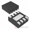
The 8-Lead WDFN package measures 2mm × 2mm and includes an exposed thermal pad for improved heat dissipation. This package is the most compact option and is preferred for applications requiring high current delivery or operation in elevated temperature environments. The WDFN package is also available for all ten voltage variants.
Thermal Management and PCB Layout Considerations for the MCP1501
Proper PCB layout is essential for achieving the specified performance of the MCP1501, particularly for load regulation and thermal management. The device should be mounted on a low-stress area of the PCB, away from edges, screw holes, and large components that might cause mechanical stress during assembly or operation. Mechanical stress can cause the output voltage to shift from its initial value, particularly in the SOT-23 package.
The power supply decoupling capacitor should be placed as close as possible to the VDD pin, ideally within 5mm. A 0.1µF ceramic capacitor is recommended for this purpose. This capacitor provides a low-impedance path for high-frequency supply noise, preventing it from reaching the reference circuit.
For applications requiring high load currents or highly variable load currents, the PCB layout becomes even more critical. The device should be grounded to a large ground plane with good thermal mass. The MCP1501 should not be placed on a small daughter card or connected to ground via long traces or single vias, as the additional power dissipation caused by high load current will cause self-heating of the device, resulting in a small change in output voltage.
For systems with high ground currents, variations in the local ground can be a source of load regulation error. These variations are usually solved by ensuring the local ground for the device is shared with the point of load. In some cases, it may be necessary to ensure the device ground is specifically kelvin-sourced from the point of load, such that zero IR-drop from unassociated circuitry is seen on the device output voltage.
In the SOIC and WDFN packages, the separate output and feedback pins can be routed separately and connected near the point of load to reduce or eliminate routing-related voltage drop. The feedback pin is the one that accurately holds the output voltage, so connecting the feedback pin directly to the point of load ensures that the load sees the correct reference voltage, even if there is trace resistance between the device output pin and the load.
Application Design and Implementation with the MCP1501
The MCP1501 is designed to integrate easily into precision analog systems, with straightforward circuit configurations and flexible application options. Proper application design ensures that the device delivers its specified performance while meeting the specific requirements of the target system.
Basic Circuit Configuration and Decoupling Requirements for the MCP1501
The basic circuit configuration for the MCP1501 is straightforward. The supply voltage is applied to the VDD pin, the output is taken from the OUT pin, and the device is grounded through the GND pin. In the SOIC and WDFN packages, the feedback pin should be connected to the output pin at the device. In the SOT-23 package, this connection is internal.
A 0.1µF ceramic capacitor should be connected between the VDD pin and ground, placed as close as possible to the device. This capacitor provides decoupling for the supply voltage, reducing high-frequency noise that might otherwise couple into the reference circuit. If the input voltage source has excessive noise, an additional 2.2µF ceramic capacitor can be added between the VDD pin and ground to provide additional low-frequency filtering.
An output capacitor is not required for stability of the voltage reference, as the MCP1501 is internally compensated for stability with capacitive loads up to 10nF. However, an output capacitor may be optionally added to provide noise filtering or to act as a charge reservoir for switching loads such as successive approximation register (SAR) analog-to-digital converters. When a SAR ADC samples the reference voltage, it draws a brief pulse of current from the reference. An output capacitor can supply this current pulse, preventing the reference voltage from drooping during the sampling period.
Output Filtering and Noise Reduction Techniques for the MCP1501
For applications where the output noise of the MCP1501 is too high, an external RC filter can be added to further reduce noise. A simple first-order low-pass filter can be implemented using a resistor and capacitor, with the cutoff frequency selected based on the application requirements. For example, a 10kΩ resistor and 1µF capacitor create a cutoff frequency of approximately 15.9 Hz, providing 20 dB/decade attenuation above this frequency.
When implementing an external filter, an op-amp buffer should be used to isolate the filter from the load. The op-amp buffer provides additional drive capability, with faster response time than the voltage reference alone. The MCP6286 operational amplifier is recommended for this application, as it offers low offset voltage and low noise characteristics compatible with precision reference applications.
The external filter approach trades off bandwidth for noise reduction. The 15.9 Hz cutoff frequency means that the reference will respond slowly to changes in supply voltage or load current. For applications where fast transient response is required, the filter cutoff frequency should be increased, reducing the noise filtering benefit. The choice of filter cutoff frequency depends on the specific application requirements.
Capacitive Load Handling and Transient Response in the MCP1501
The MCP1501 is internally compensated for stability with capacitive loads up to 10nF. This means that the device will remain stable and will not oscillate when driving a 10nF capacitive load directly. However, larger capacitors can be used if a series resistor is added between the output and the capacitor.
The series resistor limits the rate of change of current flowing into the capacitor, reducing the transient overshoot and ringing that would otherwise occur. The transient response depends on both the series resistance and the capacitive load value. For a given capacitive load, increasing the series resistance increases the settling time but reduces the overshoot. The optimal series resistance value depends on the specific application requirements.
Typical transient response measurements show that with a 4.7nF capacitive load and a 100Ω series resistor, the MCP1501 settles to within 1% of the final value in approximately 1 microsecond. With larger capacitive loads or higher series resistance values, the settling time increases proportionally.
Precision Data Acquisition System Design Using the MCP1501
Precision data acquisition systems require stable, low-noise voltage references to achieve high resolution and accuracy. The MCP1501 is well-suited for this application, providing the accuracy and stability required for high-resolution analog-to-digital converters.
ADC Reference Implementation with the MCP1501
The MCP1501 can be used as the reference voltage for analog-to-digital converters, providing the voltage scale against which the ADC measures input signals. For a 12-bit ADC with a 2.5V reference, each bit represents 610 µV. The ±0.1% accuracy of the MCP1501 ensures that the reference voltage remains within ±2.5 mV of the nominal 2.5V, corresponding to approximately ±4 LSBs of error.
The reference should be connected to the ADC reference input with short traces to minimize noise coupling. If the ADC has separate reference and reference return pins, these should be connected to the MCP1501 output and ground respectively, with the connections made as close as possible to the ADC pins.
For SAR ADCs that draw brief pulses of current during the sampling phase, an output capacitor on the reference can help maintain voltage stability. A 1µF capacitor is typically sufficient for this purpose. The capacitor should be placed close to the ADC reference input pin to minimize the inductance of the connection.
The MCP1501 can supply reference current to multiple ADCs if the total current requirement does not exceed 20 mA. However, each ADC should have its own local decoupling capacitor connected directly to its reference input pin, to prevent one ADC's sampling transients from affecting the reference voltage seen by other ADCs.
Negative Voltage Reference Generation Using the MCP1501
Applications requiring negative voltage references can use the MCP1501 in combination with an operational amplifier to generate an inverted reference. The circuit uses the MCP1501 to drive one input of an inverting amplifier configuration, with equal resistors in the input and feedback paths. The output voltage of the amplifier is equal to the negative of the MCP1501 output voltage.
For example, using an MCP1501-25 (2.5V) with an MCP6061 operational amplifier and two 10kΩ resistors produces a -2.5V output. The MCP6061 is recommended for this application due to its low offset voltage and low noise characteristics. The operational amplifier should be powered from a negative supply voltage that is at least 1V more negative than the desired output voltage.
Industrial and Automotive Applications of the MCP1501
The MCP1501 is suitable for a wide range of industrial and automotive applications where precision voltage references are required. The 6-Lead SOT-23 package is AEC-Q100 automotive qualified, enabling use in vehicle electronics such as battery management systems, motor control circuits, and sensor signal conditioning.
In battery management systems, the MCP1501 provides a stable reference for monitoring battery voltage and current. The low quiescent current of 140 µA makes it suitable for always-on monitoring circuits that must operate continuously to detect fault conditions.
In industrial control systems, the MCP1501 provides the reference voltage for precision analog-to-digital converters used in process monitoring and control. The wide operating temperature range of -40°C to +125°C enables operation in harsh industrial environments.
In medical equipment applications, the MCP1501 provides the precision reference required for patient monitoring circuits and diagnostic equipment. The low noise and high accuracy ensure that medical measurements are reliable and repeatable.
Conclusion
The MCP1501 buffered voltage reference combines precision band gap design with chopper-based amplification to deliver stable, low-drift output voltage across a wide range of operating conditions. The ±0.1% initial accuracy, 50 ppm/°C maximum temperature coefficient, and 30 µVRMS output noise make the MCP1501 suitable for precision data acquisition systems, medical equipment, industrial controls, and automotive applications. The device's ability to source and sink 20 mA of current, combined with its low quiescent current of 140 µA, provides flexibility for both high-current and battery-powered applications. Available in three package options with ten voltage variants, the MCP1501 addresses diverse system requirements while maintaining consistent performance specifications. Proper PCB layout and application circuit design are essential for achieving the specified performance, particularly for load regulation and thermal management in high-current applications.
Frequently Asked Questions (FAQ)
- Q1. What is the difference between the MCP1501 and other voltage reference devices, and when should the MCP1501 be selected over alternatives?
-
- A1. The MCP1501 is distinguished by its combination of buffered output capability (±20 mA), low temperature coefficient (50 ppm/°C maximum), and chopper-based amplifier architecture that reduces long-term drift. Unlike unbuffered references that require external buffers, the MCP1501 integrates the buffer stage, reducing component count and PCB area. The device should be selected when the application requires both precision accuracy and the ability to drive multiple loads or supply current to precision analog circuits. The chopper amplifier architecture makes the MCP1501 particularly suitable for applications requiring low long-term drift, such as precision instrumentation or systems requiring extended calibration intervals.
- Q2. How does the temperature coefficient specification of 50 ppm/°C affect system accuracy over the operating temperature range?
-
- A2. The 50 ppm/°C temperature coefficient, combined with the ±0.1% initial accuracy specification, ensures that the output voltage remains within ±0.1% across the entire -40°C to +125°C operating range. For a 2.5V reference, this means the output will remain between 2.475V and 2.525V across all temperatures. To calculate the maximum voltage change due to temperature, multiply the temperature coefficient by the temperature change and the nominal output voltage. For example, a 50°C temperature change produces a voltage change of 50 ppm/°C × 50°C × 2.5V = 6.25 mV, which is well within the ±0.1% specification. For applications operating over smaller temperature ranges, the actual voltage change will be proportionally smaller.
- Q3. What is the significance of the separate output and feedback pins in the SOIC and WDFN packages, and how should they be connected?
-
- A3. The feedback pin provides the voltage reference for the internal feedback control loop, while the output pin delivers current to the load. In ideal conditions with no trace resistance, these pins would have identical voltages. However, when load current flows through the trace connecting the output pin to the load, the trace resistance causes a voltage drop that appears on the output pin but not on the feedback pin. By connecting the feedback pin directly to the point of load (kelvin connection), the feedback loop compensates for the trace resistance, ensuring that the load sees the correct reference voltage. This technique is particularly valuable in high-current applications where trace resistance would otherwise introduce significant voltage errors. For low-current applications (less than 5 mA), the effect of trace resistance is negligible, and the output and feedback pins can be connected together at the device.
- Q4. How should the MCP1501 be decoupled, and what is the purpose of the input and output capacitors?
-
- A4. A 0.1µF ceramic capacitor should be connected between the VDD pin and ground, placed as close as possible to the device (within 5mm). This capacitor provides high-frequency decoupling for the supply voltage, reducing noise that might otherwise couple into the reference circuit. If the input voltage source has excessive noise or ripple, an additional 2.2µF ceramic capacitor can be added to provide additional low-frequency filtering. An output capacitor is not required for stability, as the MCP1501 is internally compensated for capacitive loads up to 10nF. However, an output capacitor may be added for noise filtering or to provide charge storage for switching loads such as SAR ADCs. When adding an output capacitor larger than 10nF, a series resistor should be used to maintain stability.
- Q5. What load current can the MCP1501 supply, and how does load current affect the output voltage?
-
- A5. The MCP1501 can source or sink up to 20 mA of current from its output. The load regulation specification of 40 ppm/mA indicates that for every milliampere of load current change, the output voltage will change by no more than 40 parts per million of the nominal output voltage. For a 2.5V reference, a 10 mA load current change produces a maximum voltage change of 40 ppm/mA × 10 mA × 2.5V = 1 mV. This specification assumes proper PCB layout with the device grounded to a large ground plane and the feedback pin connected to the point of load. Poor layout, such as connecting the device to ground through a single via or long trace, will degrade load regulation performance due to self-heating effects.
- Q6. How does the MCP1501 perform in battery-powered applications, and what is the typical power consumption?
-
- A6. The MCP1501 is well-suited for battery-powered applications due to its low quiescent current of 140 µA. This current is drawn continuously whenever the device is powered, regardless of whether load current is being supplied. For a system powered by a 3V battery, the MCP1501 alone consumes approximately 420 µW of power. Over a year of continuous operation, this represents approximately 3.7 mAh of battery capacity. In applications where the reference is not continuously required, the shutdown pin can be used to disable the device and reduce power consumption to near zero. However, the shutdown pin should only be used after the device has been powered up normally, allowing the internal reset circuit to release.
- Q7. What is the significance of the chopper-based amplifier architecture, and how does it improve performance compared to traditional amplifier designs?
-
- A7. The chopper-based amplifier modulates any offset errors onto a high-frequency carrier signal, then demodulates and filters these errors, leaving only the true reference signal. This technique effectively eliminates low-frequency offset drift that would otherwise increase the temperature coefficient and long-term drift of the reference. Traditional amplifiers accumulate offset errors that vary with temperature, introducing drift into the reference output. The chopper amplifier approach reduces temperature-dependent offset drift to negligible levels, enabling the MCP1501 to achieve its specified 50 ppm/°C temperature coefficient and excellent long-term drift performance. The chopping frequency is removed from the output by additional filtering circuitry, ensuring clean reference voltage delivery.
- Q8. How should the MCP1501 be used as a reference for analog-to-digital converters, and what precautions should be taken?
-
- A8. The MCP1501 output should be connected directly to the ADC reference input with short traces to minimize noise coupling. If the ADC has separate reference and reference return pins, these should be connected to the MCP1501 output and ground respectively. For SAR ADCs that draw brief pulses of current during sampling, a 1µF output capacitor placed close to the ADC reference input pin can help maintain voltage stability during the sampling transient. If multiple ADCs are referenced from a single MCP1501, each ADC should have its own local decoupling capacitor to prevent one ADC's sampling transients from affecting the reference voltage seen by other ADCs. The total load current from all ADCs must not exceed 20 mA.
- Q9. What PCB layout practices are recommended for optimal MCP1501 performance, particularly in high-current applications?
-
- A9. The device should be mounted on a low-stress area of the PCB, away from edges, screw holes, and large components. The power supply decoupling capacitor should be placed within 5mm of the VDD pin. For high-current applications, the device should be grounded to a large ground plane with good thermal mass, and should not be placed on a small daughter card or connected to ground via long traces or single vias. The feedback pin should be connected directly to the point of load (kelvin connection) to eliminate IR-drop effects on the output voltage. In systems with high ground currents, the device ground should be shared with the point of load to minimize ground potential variations. For the WDFN package, the exposed thermal pad should be grounded to improve heat dissipation.
- Q10. How can the output noise of the MCP1501 be further reduced if the specified 30 µVRMS is insufficient for the application?
-
- A10. An external RC low-pass filter can be added to the output to further reduce noise. A simple first-order filter using a 10kΩ resistor and 1µF capac