Product Overview – MCP1501 High-Precision Buffered Voltage Reference
The MCP1501 high-precision buffered voltage reference from Microchip Technology is a low-drift, bandgap-based reference capable of both sinking and sourcing up to 20 mA. Targeted at precision analog systems, MCP1501 integrates a buffer amplifier around a finely trimmed bandgap core, delivering fixed output voltages with 0.1% initial accuracy and a maximum temperature coefficient of 50 ppm/°C over a –40°C to +125°C operating range.
A chopper-stabilized amplifier architecture is used in the MCP1501 bandgap core to reduce offset and drift, keeping the output voltage stable over temperature and time. The device operates from a wide 1.65 V to 5.5 V supply (depending on variant), making it adaptable to a broad range of low-voltage and mixed-signal systems.
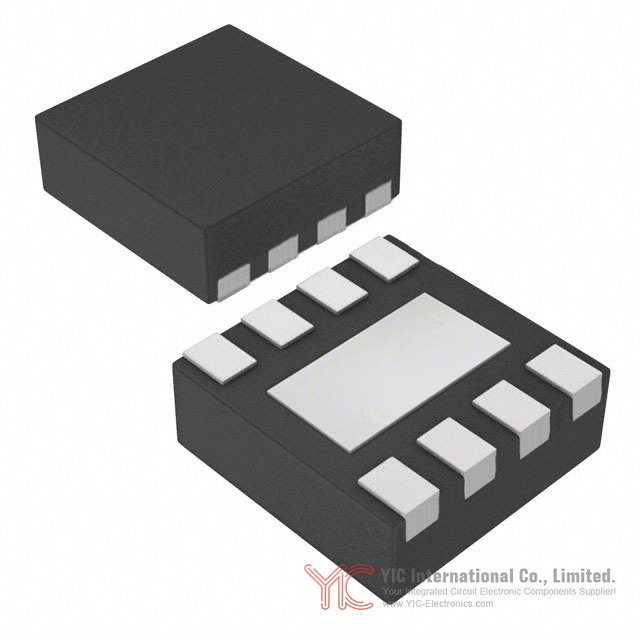
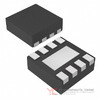
MCP1501 supports 10 fixed output voltage variants from 1.024 V to 5.000 V and is available in three package types: 6‑Lead SOT‑23 (AEC‑Q100 qualified), 8‑Lead SOIC, and 8‑Lead 2 × 2 mm WDFN with exposed pad. Output noise is typically 30 μVrms (0.1 Hz to 10 kHz), and typical no‑load supply current is 140 μA, enabling use in both precision and low-power designs.
---
2.
MCP1501 Voltage Options and Package Portfolio
The MCP1501 family offers a comprehensive set of fixed output voltages and multiple packages, allowing it to be matched to different system architectures and layout constraints.
MCP1501 fixed voltage variants
At 25°C, MCP1501 output variants are trimmed to tight limits, with typical nominal values and output ranges as follows:
- MCP1501‑10: 1.024 V (1.0230 V to 1.0250 V)
- MCP1501‑12: 1.250 V (1.2488 V to 1.2513 V)
- MCP1501‑18: 1.800 V (1.7982 V to 1.8018 V)
- MCP1501‑20: 2.048 V (2.0460 V to 2.0500 V)
- MCP1501‑25: 2.500 V (2.4975 V to 2.5025 V)
- MCP1501‑30: 3.000 V (2.9970 V to 3.0030 V)
- MCP1501‑33: 3.300 V (3.2967 V to 3.3033 V)
- MCP1501‑40: 4.096 V (4.0919 V to 4.1001 V)
- MCP1501‑45: 4.500 V (4.4955 V to 4.5045 V) – 6‑Lead SOT‑23 only
- MCP1501‑50: 5.000 V (4.9950 V to 5.0050 V) – 6‑Lead SOT‑23 only
All MCP1501 variants are specified with an initial accuracy of 0.1% at 25°C, which simplifies error budgeting in data converter and sensor front-end designs.
MCP1501 package options and AEC‑Q100 support
MCP1501 is offered in the following packages:
- MCP1501 6‑Lead SOT‑23
- Compact footprint for space-constrained designs
- Internal connection between OUT and FEEDBACK
- AEC‑Q100 qualified for automotive applications
- MCP1501 8‑Lead SOIC
- Standard footprint for ease of handling and layout
- Separate OUT and FEEDBACK pins for Kelvin‑sense connections
- MCP1501 8‑Lead 2 × 2 mm WDFN with exposed pad
- Very small area for high-density boards
- Separate OUT and FEEDBACK pins
- Exposed thermal pad (EP) that can be soldered to ground to improve thermal performance and noise immunity
The presence of both mainstream SOIC and miniature WDFN/SOT‑23 packages allows MCP1501 to serve designs ranging from rugged industrial boards to compact portable instruments.
---
3.
MCP1501 Electrical Performance and Accuracy Metrics
The MCP1501 high-precision buffered voltage reference is defined by a set of core DC characteristics that determine reference stability under changing conditions.
Supply voltage range per MCP1501 variant
The MCP1501 supply range depends on the chosen output voltage:
- MCP1501‑10, MCP1501‑12: 1.65 V to 5.5 V
- MCP1501‑18: 2.0 V to 5.5 V
- MCP1501‑20: 2.25 V to 5.5 V
- MCP1501‑25: 2.70 V to 5.5 V
- MCP1501‑30: 3.2 V to 5.5 V
- MCP1501‑33: 3.5 V to 5.5 V
- MCP1501‑40: 4.3 V to 5.5 V
- MCP1501‑45: 4.7 V to 5.5 V
- MCP1501‑50: 5.2 V to 5.5 V
These limits ensure that the internal bandgap and buffer amplifier have sufficient headroom to maintain regulation at the specified output voltage.
Temperature coefficient and drift of MCP1501
For the MCP1501 family, the maximum output temperature coefficient (TC) is specified as 50 ppm/°C. TC describes how much the reference output varies from its initial value as ambient temperature changes. It is defined as:
TC = (VOUT(MAX) − VOUT(MIN)) × 10⁶ / (ΔT × VOUT(NOM))
where VOUT(MAX) and VOUT(MIN) are the maximum and minimum output voltage over the specified temperature range ΔT, and VOUT(NOM) is the nominal output.
For example, if VOUT drifts by 2 mV over a 100°C span at a 2.048 V nominal value, TC is roughly:
TC ≈ (2 mV × 10⁶) / (100°C × 2.048 V) ≈ 9.8 ppm/°C
This kind of calculation helps quantify the MCP1501 contribution to system accuracy across temperature.
MCP1501 line regulation and supply sensitivity
Line regulation for MCP1501 is defined as the change in output voltage versus change in input voltage:
Line Regulation (%) = (ΔVOUT / ΔVIN) × 100%
It can also be expressed as ppm/V:
Line Regulation (ppm/V) = (ΔVOUT / VOUT(NOM)) × 10⁶ / ΔVIN
For MCP1501, the maximum line regulation is specified as 50 ppm/V, with typical performance around 5 ppm/V. This means that a 1 V change in supply would cause up to 50 ppm of relative change in VOUT at the worst case.
As an example, for MCP1501‑20 (2.048 V output), a 250 mV change in VIN producing 2 μV change at VOUT corresponds to approximately:
(2 μV / 2.048 V) × 10⁶ / 0.25 V ≈ 3.9 ppm/V
Such behavior supports stable reference performance even when supply rails vary within their specified range.
MCP1501 load regulation and dropout behavior
MCP1501 specifies load regulation under both sinking and sourcing conditions:
- Load regulation, sinking current: 10 ppm/mA typical, 40 ppm/mA maximum (–5 mA < ILOAD < 0)
- Load regulation, sourcing current: 15 ppm/mA typical, 70 ppm/mA maximum (0 < ILOAD < +5 mA)
This quantifies how VOUT changes when the load current varies, which is key when the reference directly feeds high-resolution ADCs or DACs with varying input loads.
Dropout voltage for MCP1501 is defined as the difference between VDD and VOUT at 5 mA load current:
VDO ≈ 200 mV (–5 mA < ILOAD < +5 mA)
This indicates that the supply voltage must exceed the desired output by at least approximately 200 mV to maintain regulation under stated load conditions.
---
4.
MCP1501 Power, Noise and Temperature Characteristics
The MCP1501 high-precision buffered voltage reference combines low power consumption with low noise and wide temperature capability.
MCP1501 supply current and shutdown behavior
Typical operating current for MCP1501 at no load is:
- IDD (typical): 140 μA
- IDD (maximum): 350 μA at 25°C, 550 μA over temperature
In Shutdown mode, the MCP1501 shutdown current is approximately 205 nA (typical at 25°C). All device options share this low shutdown current level.
A digital SHDN pin (active low) is used to disable the output. The device should first power up normally; once fully powered, the SHDN pin can be asserted low to place MCP1501 into Shutdown, during which the output driver and feedback are tri-stated.
MCP1501 output noise characteristics
Noise performance directly impacts the resolution and repeatability of data acquisition systems. MCP1501 output noise is specified as:
- MCP1501‑10:
- 18 μVPP, 0.1 Hz to 10 Hz
- 30 μVrms, 0.1 Hz to 10 kHz
- MCP1501‑40 (representative high-voltage variant):
- 57 μVPP, 0.1 Hz to 10 Hz
- 97 μVrms, 0.1 Hz to 10 kHz
Peak-to-peak noise (VPP) is approximately six times VRMS (VPP ≈ 6 × VRMS), consistent with Gaussian noise assumptions. Such low noise levels are a match for high-resolution ADCs and DACs, preventing the reference from becoming the dominant noise source.
MCP1501 output voltage hysteresis
MCP1501 specifies an output voltage hysteresis of about 300 μV. Hysteresis refers to the difference in VOUT when temperature or operating conditions are cycled, and then returned to the same point. This parameter helps anticipate small residual shifts in reference voltage after thermal cycling or repeated operating mode changes.
MCP1501 temperature ranges and thermal resistance
MCP1501 is specified over an extended operating temperature range:
- Operating ambient temperature (TA): –40°C to +125°C
- Storage temperature: –65°C to +150°C
Typical junction-to-ambient thermal resistance values:
- SOT‑23‑6: θJA ≈ 190.5°C/W
- SOIC‑8: θJA ≈ 149.5°C/W
- DFN‑8 (2 × 2 mm WDFN): θJA ≈ 141.3°C/W
For the WDFN package, the exposed pad can be soldered to the PCB ground plane to reduce thermal impedance and improve thermal stability of the MCP1501 reference.
---
5. MCP1501 Pin Functions and System-Level Behavior
Understanding MCP1501 pin functions is central to designing robust reference circuits.
MCP1501 buffered output (OUT)
The OUT pin is the buffered voltage reference output of MCP1501. In the SOIC and WDFN packages, OUT is separate from FEEDBACK and must be externally connected to the FEEDBACK pin at the device location. This configuration permits Kelvin-sensing to compensate for PCB trace resistance and IR drops.
In Shutdown mode, both the output driver and FEEDBACK are placed into a high-impedance state.
MCP1501 feedback pin (FEEDBACK) and Kelvin connection
The FEEDBACK pin in MCP1501 is the input to the buffer amplifier that senses the reference output voltage:
- In 8‑Lead SOIC and 2 × 2 mm WDFN, FEEDBACK is a separate pin. The output is regulated such that the FEEDBACK pin precisely holds the specified reference voltage. Any voltage drop between OUT and FEEDBACK (due to series resistance in traces or connectors) is effectively corrected.
- In 6‑Lead SOT‑23, the FEEDBACK connection is internal; the user only accesses the OUT pin.
For applications with significant load current or longer traces, placing the FEEDBACK pin at the load side (Kelvin connection) allows MCP1501 to maintain accurate output at the point of load rather than at the IC pin. For instance, in a high-current ADC input reference path, routing FEEDBACK to the ADC reference pin and OUT through a dedicated trace helps remove the effect of trace resistance on reference accuracy.
MCP1501 system ground (GND) and exposed pad (EP)
Multiple GND pins are provided in MCP1501 packages:
- SOT‑23‑6: Pins 2, 3, 5 – system ground
- SOIC‑8 and WDFN‑8: Pins 2, 4, 5, 6 – system ground
These grounds should be connected to the system ground plane, with short, low-impedance connections to minimize noise coupling.
For the WDFN package, the exposed pad (EP) is not internally connected but grounding it is recommended. Soldering EP to the PCB ground plane increases thermal dissipation and can improve EMC behavior by adding a larger, low-impedance ground area near the MCP1501.
MCP1501 power supply input (VDD) and start-up thresholds
The VDD pin is both power input and the input voltage for the MCP1501 internal reference circuitry. A 0.1 μF bypass capacitor should be placed as close as possible to the VDD pin and ground to suppress supply transients and noise.
Start-up behavior includes:
- Power-on reset release voltage (VPOR): about 1.45 V (typical) on rising VDD
- Power-on reset rearm voltage: approximately 0.8 V (typical) on falling VDD
On rising VDD, MCP1501 internal circuits remain in reset until the supply exceeds VPOR, ensuring that the output only becomes valid once the internal reference is stable. When VDD drops, driving it below the reset rearm voltage ensures that the device properly resets before the next power-up.
MCP1501 shutdown pin (SHDN) and logic thresholds
The SHDN pin in MCP1501 is an active-low digital input used to enable or disable the reference:
- When SHDN is low, the device enters Shutdown; the output is disabled, and the output and feedback are tri-stated.
- When SHDN is high, MCP1501 operates normally.
Typical logic thresholds at VDD = 5.5 V:
- VL (low threshold): around 1.35 V
- VH (high threshold): around 3.80 V
The device should be fully powered up (VDD above VPOR and internal circuits settled) before SHDN is used for dynamic control. This allows designers to power up the system in a known state and then apply SHDN to manage power consumption.
---
6.
MCP1501 Application Scenarios and Design Examples
The MCP1501 high-precision buffered voltage reference lends itself to a wide range of precision analog applications due to its accuracy, low noise, and sourcing/sinking capability.
Data acquisition and converter references with MCP1501
In precision data acquisition systems and high-resolution data converters (ADCs and DACs), MCP1501 can be used as the primary reference:
- MCP1501‑10 (1.024 V) and MCP1501‑20 (2.048 V) are well suited for ADCs requiring binary-scaled references (e.g., 1.024 V for 10-bit or 12-bit converters, 2.048 V for 12‑bit or 16‑bit ADCs with standard full-scale ranges).
- MCP1501‑25 (2.5 V) and MCP1501‑50 (5.0 V) fit many DAC and ADC reference inputs in industrial and instrumentation applications.
For example, in a 16-bit ADC with 2.048 V full-scale, a reference drift of 50 ppm/°C corresponds to a drift of about 0.1 LSB/°C, supporting stable measurement accuracy over several tens of degrees without frequent recalibration.
Medical and industrial equipment using MCP1501
MCP1501 is specified for industrial controls and medical equipment applications where repeatable measurements over temperature and time are required. The temperature range of –40°C to +125°C, low drift, and good load regulation permit use in:
- Sensor signal-conditioning front ends
- Programmable logic controllers (PLCs)
- Patient monitoring devices and medical instruments with precision analog chains
Electric vehicle battery management with MCP1501
MCP1501 is also suited to electric vehicle battery management systems (BMS). The AEC‑Q100 qualification of the SOT‑23 package supports automotive-grade designs, while the –40°C to +125°C range aligns with automotive environments.
In a BMS, MCP1501 can provide a reference for:
- Analog front-end ICs measuring cell voltages and currents
- Calibration circuits for current sense amplifiers
- Reference rails for MCU ADCs that supervise battery health
Battery-powered and low-power devices with MCP1501
For battery-powered devices, MCP1501 offers:
- Low supply current (typical 140 μA)
- Shutdown current ~205 nA
- Wide operating voltage down to 1.65 V for low-voltage variants
These attributes enable MCP1501 to serve as a precision reference while contributing minimally to the overall power budget, especially when SHDN is used to disable the reference between measurement cycles.
Kelvin-sense example using MCP1501 WDFN
In a high-current, low-voltage design where MCP1501 WDFN is used to supply a 3.3 V reference to a DAC, the OUT pin can be routed through a trace to the DAC board area, while the FEEDBACK pin is routed separately and directly to the DAC reference input pin. If the trace between OUT and the DAC has a small resistance and carries several milliamps, any IR drop along that trace is compensated because MCP1501 regulates the voltage at FEEDBACK, not merely at the OUT pin. This ensures that the DAC sees the intended 3.3 V, irrespective of trace voltage drop.
---
7.
MCP1501 Practical Selection and Implementation Considerations
Practical use of the MCP1501 high-precision buffered voltage reference involves selecting the appropriate variant, package, and configuration for the target system.
Choosing the right MCP1501 voltage variant
Selection typically proceeds from system reference requirements:
- Binary-related references (1.024 V, 2.048 V, 4.096 V) for high-resolution ADCs
- Round values (1.250 V, 2.5 V, 3.3 V, 5.0 V) for communication with sensor and logic domains
- Higher voltages (4.5 V, 5.0 V) where reference must match or track supply rails in legacy or 5 V systems
The chosen MCP1501 variant must be compatible with the system supply voltage. For example, MCP1501‑50 requires a supply in the 5.2 V to 5.5 V range, whereas MCP1501‑10 can operate from 1.65 V upward.
Package selection for MCP1501
Package choice depends on area constraints, assembly flow, and environmental conditions:
- MCP1501 SOT‑23 (AEC‑Q100): For automotive and space-limited boards, where Kelvin-sense is not required.
- MCP1501 SOIC‑8: For prototyping, laboratory equipment, and designs preferring larger pad pitch.
- MCP1501 WDFN‑8 (2 × 2 mm): For dense or portable systems needing lower thermal resistance; the exposed pad can be tied to ground.
Power supply decoupling and layout for MCP1501
For stable operation:
- Place a 0.1 μF ceramic capacitor close to VDD and GND of MCP1501.
- Use a solid ground plane and short, wide traces to the GND pins.
- For WDFN, connect the exposed pad to the ground plane through multiple vias.
Kelvin-sense layout with MCP1501 FEEDBACK
When using MCP1501 SOIC or WDFN:
- Route FEEDBACK as a separate trace directly to the voltage point where accuracy is required (e.g., ADC reference pin).
- Keep FEEDBACK away from noisy digital lines to minimize coupling.
- OUT trace can be wider to carry load current; FEEDBACK trace carries negligible current and is used purely for sensing the actual voltage.
Managing shutdown and start-up of MCP1501
When using SHDN:
- Ensure MCP1501 is allowed to reach its normal operating state after power-on (VDD above VPOR, internal reset released) before toggling SHDN.
- Use appropriate pull-up/pull-down resistors on SHDN to guarantee a defined state in the absence of MCU drive.
- In systems that power-cycle frequently, ensure VDD falls below the specified reset rearm voltage so MCP1501 fully resets before re-energizing.
---
8.
Conclusion – Design Value of the MCP1501 Family
The MCP1501 high-precision buffered voltage reference combines 0.1% initial accuracy, a maximum 50 ppm/°C temperature coefficient, and low noise with the ability to source and sink up to 20 mA across a wide –40°C to +125°C range. The family’s 10 fixed voltage options from 1.024 V to 5.000 V, together with SOT‑23, SOIC, and 2 × 2 mm WDFN packages, allow straightforward alignment to a wide variety of precision analog architectures.
Features such as low supply current, ultra-low shutdown current, Kelvin-sense FEEDBACK routing in SOIC and WDFN packages, and AEC‑Q100 qualification for the SOT‑23 variant position MCP1501 as a versatile reference solution in data acquisition, medical and industrial equipment, battery-powered devices, and electric vehicle battery management systems.
By understanding MCP1501 parameters such as line and load regulation, dropout voltage, noise performance, and pin functions, designers can integrate the MCP1501 family into their systems with predictable and stable reference behavior, simplifying error budgets and long-term performance planning.
---
Frequently Asked Questions (FAQ)
- Q1. What output voltage options are available in the MCP1501 family?
-
- A1. MCP1501 offers ten fixed output voltage options:
- MCP1501‑10: 1.024 V
- MCP1501‑12: 1.250 V
- MCP1501‑18: 1.800 V
- MCP1501‑20: 2.048 V
- MCP1501‑25: 2.500 V
- MCP1501‑30: 3.000 V
- MCP1501‑33: 3.300 V
- MCP1501‑40: 4.096 V
- MCP1501‑45: 4.500 V (SOT‑23 only)
- MCP1501‑50: 5.000 V (SOT‑23 only)
Each variant is factory trimmed to 0.1% initial accuracy at 25°C. - Q2. Which supply voltage ranges are compatible with each MCP1501 variant?
-
- A2. The supply voltage ranges for MCP1501 variants are:
- MCP1501‑10, MCP1501‑12: 1.65 V to 5.5 V
- MCP1501‑18: 2.0 V to 5.5 V
- MCP1501‑20: 2.25 V to 5.5 V
- MCP1501‑25: 2.70 V to 5.5 V
- MCP1501‑30: 3.2 V to 5.5 V
- MCP1501‑33: 3.5 V to 5.5 V
- MCP1501‑40: 4.3 V to 5.5 V
- MCP1501‑45: 4.7 V to 5.5 V
- MCP1501‑50: 5.2 V to 5.5 V
Selection must ensure that the chosen VDD range is available in the target system. - Q3. How accurate is the MCP1501 output over temperature?
-
- A3. MCP1501 specifies:
- Initial accuracy: 0.1% at 25°C
- Maximum temperature coefficient: 50 ppm/°C over –40°C to +125°C
This means output drift with temperature is limited to approximately 0.005% per 10°C change, enabling high accuracy across wide temperature ranges when combined with system-level calibration if required. - Q4. How much current can the MCP1501 source and sink?
-
- A4. MCP1501 can typically source and sink up to ±20 mA load current at 25°C while maintaining its specified regulation. Load regulation is 10 ppm/mA typical (sinking) and 15 ppm/mA typical (sourcing). This capability allows MCP1501 to directly drive reference loads such as ADCs, DACs, or small analog circuits without a separate buffer.
- Q5. What is the dropout voltage of MCP1501 and how does it affect system design?
-
- A5. MCP1501 dropout voltage is approximately 200 mV for load currents in the –5 mA to +5 mA range. This means VDD must exceed VOUT by roughly 200 mV for the reference to maintain regulation at the specified load. In applications running close to the minimum supply, designers should ensure sufficient supply headroom above the target reference voltage.
- Q6. How low is the noise of MCP1501 and what bandwidths are specified?
-
- A6. MCP1501 specifies output noise in two standard bandwidths:
- For MCP1501‑10 (1.024 V): 18 μVPP from 0.1 Hz to 10 Hz, and 30 μVrms from 0.1 Hz to 10 kHz.
- For MCP1501‑40 (4.096 V): 57 μVPP from 0.1 Hz to 10 Hz, and 97 μVrms from 0.1 Hz to 10 kHz.
Peak-to-peak noise is about six times the RMS value. These low noise levels support high-resolution data converters where reference noise must be well below the converter’s LSB size. - Q7. How should the FEEDBACK pin on MCP1501 SOIC and WDFN packages be connected?
-
- A7. For MCP1501 SOIC‑8 and WDFN‑8:
- In simple layouts, OUT and FEEDBACK should be shorted together at the device to create a local feedback loop.
- In precision or high-current designs, FEEDBACK can be connected to the remote load node (such as an ADC reference pin) to implement Kelvin sensing. This allows MCP1501 to regulate the voltage at the load, compensating for voltage drops along the output trace.
For the SOT‑23 package, FEEDBACK is internally connected to OUT and no external connection is required. - Q8. What is the function of the SHDN pin on MCP1501 and how should it be used?
-
- A8. SHDN is an active-low shutdown pin on MCP1501:
- When SHDN is driven low, MCP1501 enters Shutdown; the output driver and FEEDBACK are tri-stated, and the supply current drops to around 205 nA (typical at 25°C).
- When SHDN is high, MCP1501 operates normally.
The device should be powered up first (VDD above VPOR and internal reset released) before toggling SHDN. In systems where power cycling and reference control are handled by a microcontroller, SHDN can be driven from a GPIO to reduce power consumption between measurement intervals. - Q9. How does MCP1501 handle power-on reset and under-voltage conditions?
-
- A9. MCP1501 contains an internal reset circuit. Key parameters are:
- Power-on reset release voltage (VPOR) on rising VDD: approximately 1.45 V (typical), at which internal reset is released and the output becomes valid.
- Reset rearm voltage on falling VDD: about 0.8 V (typical). When VDD falls below this value, MCP1501 internal reset re-engages.
For reliable power cycling, VDD should be allowed to fall below the reset rearm voltage before rising again, ensuring that MCP1501 always starts from a defined reset state. - Q10. What thermal performance can be expected from MCP1501 in various packages?
-
- A10. MCP1501 typical junction-to-ambient thermal resistance values are:
- SOT‑23‑6: θJA ≈ 190.5°C/W
- SOIC‑8: θJA ≈ 149.5°C/W
- WDFN‑8 (2 × 2 mm): θJA ≈ 141.3°C/W
In the WDFN package, the exposed pad can be soldered to the PCB ground plane to further reduce thermal resistance. Although MCP1501 dissipates relatively little power (low supply current and moderate load currents), proper thermal design supports stable operation over the full –40°C to +125°C temperature range. - Q11. Is the MCP1501 suitable for automotive and EV battery management systems?
-
- A11. MCP1501 is suitable for automotive and EV battery management systems, particularly in its 6‑Lead SOT‑23 package, which is AEC‑Q100 qualified. The device’s operating temperature range of –40°C to +125°C, low temperature coefficient, and robust sourcing/sinking capability allow it to act as a reference for battery monitoring ICs, ADCs in a BMS, and other automotive precision analog functions.
- Q12. How should decoupling and grounding be implemented for MCP1501?
-
- A12. For stable and low-noise operation:
- Place a 0.1 μF ceramic capacitor between VDD and GND as close as possible to MCP1501.
- Connect all GND pins to a solid ground plane using short traces; multiple ground pins should be tied together on the PCB.
- In the WDFN package, connect the exposed pad (EP) to ground, ideally using multiple vias to the main ground plane.
This layout approach helps minimize noise coupling into the reference and improves thermal performance. - Q13. Can MCP1501 be used with battery-powered systems requiring ultra-low standby current?
-
- A13. Yes. MCP1501 typical operating current is about 140 μA with no load, and the Shutdown mode current is approximately 205 nA at 25°C. In a battery-powered system, MCP1501 can be enabled only during measurement windows via SHDN, keeping standby current to sub-microampere levels. The wide input voltage range of selected variants also aligns with common battery voltages and regulated rails.
- Q14. What are the absolute maximum ratings for MCP1501 that must not be exceeded?
-
- A14. MCP1501 absolute maximum ratings include:
- Maximum VDD: 5.5 V
- Maximum current into VDD: 30 mA
- Clamp current for pins driven outside 0 V to VDD: ±20 mA
- Maximum output current from OUTPUT pin: 30 mA
- ESD robustness (HBM: 2 kV, CDM: 1.5 kV, MM: 200 V)
Operating MCP1501 beyond these ratings can cause permanent damage. Normal operation should remain within the operating conditions specified in the electrical characteristics tables. - Q15. What line and load regulation performance can be expected from MCP1501 in practice?
-
- A15. MCP1501 typical and maximum specifications are:
- Line regulation: 5 ppm/V typical, 50 ppm/V maximum across VDD(MIN) to 5.5 V.
- Load regulation:
- Sinking: 10 ppm/mA typical, 40 ppm/mA maximum for –5 mA < ILOAD < 0
- Sourcing: 15 ppm/mA typical, 70 ppm/mA maximum for 0 < ILOAD < +5 mA
In practice, this means that moderate variations in supply and load current produce small, predictable changes in VOUT, supporting stable system performance even when the power rail or reference load is not perfectly constant.