Product Overview of the MCP1501 Series
The MCP1501 is a buffered voltage reference integrated circuit manufactured by Microchip Technology, designed to deliver stable, precision reference voltages across a wide range of industrial and commercial applications. This device represents a fundamental building block in precision measurement systems, providing a low-drift, low-noise output that serves as the foundation for accurate analog-to-digital conversion, data acquisition, and signal conditioning circuits.
The MCP1501 operates as a band gap-based voltage reference with integrated output buffering capability, enabling it to both source and sink up to 20 mA of load current. This combination of precision voltage generation and current-driving capability distinguishes the MCP1501 from simpler reference architectures, making it suitable for applications requiring both accuracy and practical drive capability.
Core Architecture and Operating Principles of the MCP1501
The MCP1501 employs a second-order temperature-compensated band gap circuit architecture that forms the foundation of its precision performance. The band gap topology works by combining two voltage sources with opposite temperature coefficients, resulting in a composite output voltage that remains relatively independent of temperature variations.
The internal design of the MCP1501 incorporates several advanced techniques to achieve its specified performance. A chopper-based amplifier architecture operates within the device to reduce temperature-dependent offsets that would otherwise degrade the temperature coefficient. This chopper amplification approach effectively reduces drift to near-zero levels by continuously sampling and correcting offset errors. Additional filtering circuitry removes the chopping frequency from the output, ensuring clean reference voltage delivery to external circuits.
Following the band gap voltage generation and temperature compensation, the reference voltage undergoes attenuation to reach the desired output level, then passes through a buffering stage that provides the output drive capability. This buffered architecture allows the MCP1501 to maintain output voltage accuracy even when delivering current to external loads, a characteristic that distinguishes buffered references from unbuffered alternatives.
Pin Configuration and Functional Description of the MCP1501
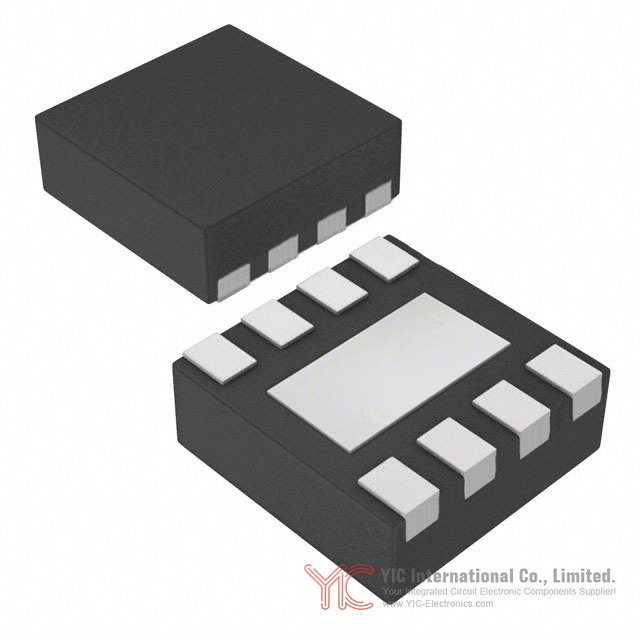
The MCP1501 is available in three package options: 6-lead SOT-23, 8-lead SOIC, and 8-lead WDFN (2 mm × 2 mm). Each package variant serves different application requirements, with the SOT-23 package offering the smallest footprint for space-constrained designs, while the SOIC and WDFN packages provide additional functionality through separate output and feedback pins.
The power supply input pin (VDD) accepts the supply voltage that powers the reference circuit and simultaneously serves as the input voltage source for the voltage reference generation. The device requires a 0.1 μF bypass capacitor connected very close to the VDD pin to filter high-frequency noise and ensure stable operation.
The buffered reference output (OUT) pin delivers the precision voltage to external circuits. On WDFN and SOIC packages, this pin should be connected to the feedback pin at the device. This connection is internal on the SOT-23 package, simplifying the circuit layout for applications using that package variant.
The feedback pin (FEEDBACK) on WDFN and SOIC packages serves as the input to the internal buffer amplifier's feedback network. By connecting this pin to the output pin at the device, the buffer amplifier maintains accurate output voltage regulation. In applications with significant PCB trace impedance or interconnect resistance between the device and load, the feedback pin can be routed separately to the point of load, effectively removing IR-drop effects on the output voltage caused by PCB resistance.
The shutdown pin (SHDN) provides digital control over device operation. This active-low input places the device into a low-power shutdown state when pulled low, with both the output driver and feedback path tristated. The device must be fully powered up before the shutdown function is used.
The system ground pin (GND) connects to the power supply return and system ground. The exposed thermal pad (EP) on WDFN packages is not internally connected but should be grounded to the PCB for thermal management purposes.
Electrical Performance Specifications of the MCP1501
The MCP1501 series offers ten voltage output options: 1.024V, 1.250V, 1.800V, 2.048V, 2.500V, 3.000V, 3.300V, 4.096V, 4.500V, and 5.000V. The 4.500V and 5.000V options are available exclusively in the 6-lead SOT-23 package.
Initial accuracy represents the output voltage tolerance at room temperature (25°C) under specified conditions. The MCP1501 achieves 0.1% initial accuracy across all voltage options, meaning the actual output voltage will be within 0.1% of the nominal specified value when the device is first powered up at room temperature.
The device operates across an extended temperature range from -40°C to +125°C, accommodating applications in harsh industrial environments, automotive systems, and outdoor installations. The operating supply voltage range varies by specific device variant but generally spans from approximately 2.7V to 5.5V, providing flexibility in system integration.
The typical operating current consumption is 140 μA, making the MCP1501 suitable for battery-powered applications where power efficiency is a design consideration. This low quiescent current allows the reference to operate continuously in portable and remote measurement systems without excessive battery drain.
The device can source or sink up to 20 mA of output current, enabling it to drive moderate loads directly without requiring additional buffer amplification. The maximum output current specifications indicate that the device can sink up to 30 mA and source up to 30 mA under absolute maximum conditions, though continuous operation should remain within the 20 mA specification.
Temperature Stability and Drift Characteristics of the MCP1501
Temperature coefficient represents one of the most significant performance metrics for precision voltage references. The MCP1501 achieves a maximum temperature coefficient of 50 ppm/°C across the full operating temperature range from -40°C to +125°C. This specification indicates that the output voltage will change by no more than 50 parts per million per degree Celsius of temperature change.
To understand the practical significance of this specification, consider a 2.048V reference with a 50 ppm/°C temperature coefficient. Over a 100°C temperature excursion, the maximum output voltage change would be approximately 10.24 mV, or about 0.5% of the nominal output voltage. This level of stability allows the MCP1501 to maintain measurement accuracy across wide temperature ranges without requiring temperature compensation in the external measurement circuit.
The temperature coefficient is measured using a specific calculation methodology. The output voltage is measured at three temperature points: the lower operating limit (-40°C), room temperature (+25°C), and the upper operating limit (+125°C). The temperature coefficient is then calculated as the maximum voltage deviation from the best-fit line through these three points, divided by the temperature range and the nominal output voltage, expressed in ppm/°C.
Long-term drift represents the gradual change in output voltage over extended periods at constant temperature. The MCP1501 exhibits minimal long-term drift, with measurements showing stable output voltage over thousands of hours at room temperature. This characteristic ensures that systems using the MCP1501 maintain calibration accuracy over the operational lifetime of the equipment.
Output voltage hysteresis describes the difference in output voltage at room temperature after the device has been cycled through the full operating temperature range. The MCP1501 demonstrates low hysteresis, meaning the output voltage returns very close to its original value after temperature cycling, indicating excellent long-term stability and minimal permanent drift from thermal stress.
Output Regulation Performance of the MCP1501
Line regulation characterizes how well the MCP1501 maintains constant output voltage when the input supply voltage changes. The MCP1501 achieves a maximum line regulation of 50 ppm/V, meaning that for every volt of input voltage change, the output voltage will change by no more than 50 parts per million of the nominal output voltage.
To illustrate this specification with a practical example, consider a 2.048V reference with 50 ppm/V line regulation. If the input supply voltage changes by 1 volt, the output voltage will change by approximately 102.4 μV. This excellent line regulation allows the MCP1501 to maintain output accuracy even in systems with noisy or varying power supplies, reducing the need for extensive input filtering.
Load regulation describes the output voltage change when the load current changes from zero to maximum. The MCP1501 achieves a maximum load regulation of 40 ppm/mA, indicating that for every milliamp of additional load current drawn from the output, the output voltage will change by no more than 40 parts per million of the nominal output voltage.
Using the same 2.048V reference example, if the load current increases by 10 mA, the output voltage will change by approximately 8.19 μV. This low load regulation allows the MCP1501 to maintain stable reference voltage even when the load current varies significantly, a characteristic particularly valuable in systems with switching loads such as successive approximation register (SAR) analog-to-digital converters.
The dropout voltage represents the minimum voltage difference required between the input supply and the output voltage for the device to maintain regulation. Under a 5 mA load condition, the MCP1501 requires approximately 0.5V of headroom, meaning the input supply must be at least 0.5V higher than the desired output voltage. This relatively low dropout voltage allows the device to operate from lower supply voltages than many alternative reference designs.
Power Supply Rejection Ratio (PSRR) measures how effectively the MCP1501 rejects noise and ripple on the input supply from appearing on the output. The PSRR varies with frequency, with the device providing excellent rejection at low frequencies and gradually decreasing rejection at higher frequencies. At low frequencies (below 100 Hz), the PSRR exceeds 80 dB, meaning input noise is attenuated by a factor of 10,000. At higher frequencies (above 10 kHz), the PSRR decreases to approximately 40-50 dB, still providing significant noise rejection.
Power Supply Requirements and Operating Conditions of the MCP1501
The MCP1501 requires a stable power supply voltage applied to the VDD pin. The minimum supply voltage varies by specific device variant but typically ranges from 2.7V to 3.0V, depending on the output voltage option selected. The maximum supply voltage is 5.5V for all variants.
The device includes an internal power-on reset circuit that ensures proper initialization when power is first applied. On a rising supply voltage, the internal reset is released when the supply reaches approximately 1.3V. On a falling supply voltage, the internal reset circuit activates when the supply drops below approximately 1.2V. For proper reset operation when power is removed, it is recommended to bring the supply voltage below 1.2V.
A 0.1 μF ceramic capacitor should be connected directly to the VDD pin, placed as close as possible to the device pins. This bypass capacitor filters high-frequency noise on the power supply and provides charge storage for transient current demands. If the input voltage source contains excessive noise, an optional 2.2 μF ceramic capacitor can be added to the input to provide additional filtering at frequencies around 1-2 MHz.
The device can be placed into shutdown mode by pulling the shutdown pin low. In shutdown, the output driver and feedback path are tristated, reducing power consumption to minimal levels. However, the device must be fully powered up and operational before the shutdown function is used. Once the device is in shutdown, it can be brought back to normal operation by releasing the shutdown pin to a high state.
Package Options and Physical Specifications of the MCP1501
The 6-lead SOT-23 package offers the smallest physical footprint, measuring approximately 3.0 mm × 2.9 mm with a height of 1.3 mm. This package is AEC-Q100 qualified for automotive applications, making it suitable for vehicle-based measurement and control systems. The SOT-23 package has the output and feedback pins internally connected, simplifying circuit design for applications that do not require separate routing of these signals.
The 8-lead SOIC package provides a larger footprint (approximately 3.9 mm × 5.0 mm) with a height of 1.75 mm. This package offers separate output and feedback pins, allowing advanced PCB layout techniques to minimize voltage drop effects. The SOIC package is widely used in industrial and commercial applications where space is less constrained than in portable or automotive designs.
The 8-lead WDFN package (2 mm × 2 mm) represents a compact alternative to the SOIC, offering a smaller footprint while maintaining the separate output and feedback pin configuration. The WDFN package includes an exposed thermal pad for improved heat dissipation, making it suitable for applications with higher load currents or thermal constraints. The WDFN package measures 2.0 mm × 2.0 mm with a height of 0.8 mm, providing excellent thermal performance in a compact form factor.
Application Circuit Design with the MCP1501
The basic application circuit for the MCP1501 consists of the device itself with power supply connections and minimal external components. The VDD pin connects to the system power supply through a 0.1 μF bypass capacitor placed very close to the device. The output pin connects to the feedback pin on WDFN and SOIC packages, or this connection is internal on the SOT-23 package. The GND pin connects to system ground, and the output is available at the OUT pin for connection to external circuits.
An output capacitor is not required for stability of the voltage reference but may be optionally added to provide noise filtering or act as a charge reservoir for switching loads. When an output capacitor is used, the maximum capacitive load without series resistance is 10 nF. Larger capacitors can be implemented if a resistor is placed in series with the capacitor to limit transient current and prevent oscillation.
For applications requiring lower output noise than the MCP1501 provides directly, an external RC low-pass filter combined with an op-amp buffer can reduce output noise. A typical filter configuration uses a 10 kΩ resistor and 1 μF capacitor to create a first-order low-pass filter with a cutoff frequency of approximately 15.9 Hz and an attenuation slope of 20 dB/decade. An op-amp such as the MCP6286 can buffer this filter output, providing additional drive capability and isolating the filter loading from the remainder of the circuit.
The MCP1501 can be configured to generate negative voltage references using an inverting amplifier circuit. In this configuration, the MCP1501 output drives one input of an inverting amplifier through a resistor, with the amplifier's non-inverting input biased to ground. A feedback resistor of equal value to the input resistor creates an inverting gain of -1, producing an output voltage equal to the negative of the MCP1501 reference voltage. For example, an MCP1501-25 (2.5V) configured this way produces a -2.5V output.
The MCP1501 serves as a precision reference for analog-to-digital converters in data acquisition systems. In a typical ADC application, the MCP1501 output connects to the reference input of the ADC, providing the voltage scale for analog-to-digital conversion. The reference voltage determines the full-scale input range of the ADC, so the precision and stability of the MCP1501 directly impact the accuracy of the digitized measurements.
For successive approximation register (SAR) ADCs, which draw variable current during the conversion process, the MCP1501's ability to source and sink 20 mA of current proves valuable. An optional output capacitor can be added to provide charge storage during conversion cycles, reducing the voltage droop on the reference during high-current transients.
PCB Layout Considerations for the MCP1501
Proper printed circuit board layout significantly impacts the performance of the MCP1501, particularly for applications requiring optimized load regulation and minimal output voltage variation. The device should be mounted on a large ground plane with good thermal mass to minimize self-heating effects that can cause output voltage changes under high load current conditions.
The MCP1501 should not be placed on small daughter cards or connected to ground through long traces or single vias if load regulation optimization is required. The additional power dissipation caused by high load current can cause self-heating of the device, resulting in small changes to the output voltage. Mounting the device directly on the main PCB with multiple vias connecting to the ground plane provides the best thermal performance.
For systems with high ground currents, variations in the local ground potential can become a source of load regulation error. These effects are minimized by ensuring the local ground for the device is shared with the point of load. In some cases, it may be necessary to implement Kelvin sourcing, where the device ground is specifically routed from the point of load such that zero IR drop from unassociated circuitry appears on the device output voltage.
On WDFN and SOIC packages, the separate output and feedback pins provide an opportunity to optimize PCB layout for high-current applications. If these pins are shorted together on the PCB adjacent to the device, any trace impedance between the device and the load will cause a small voltage drop. By routing these pins separately and connecting them near the point of load, trace-related voltage drop can be reduced or eliminated.
Mechanical stress from PCB mounting can cause the output voltage to shift from its initial value. Devices in the SOT-23 package are generally more prone to assembly stress than devices in the WDFN package. To reduce stress-related output voltage shifts, the reference should be mounted on low-stress areas of the PCB, away from PCB edges, screw holes, and large components that might flex during assembly or thermal cycling.
Conclusion
The MCP1501 represents a mature, well-characterized precision voltage reference solution suitable for a broad range of measurement and control applications. Its combination of 0.1% initial accuracy, 50 ppm/°C temperature coefficient, low output noise, and integrated output buffering capability makes it a practical choice for systems requiring stable reference voltages without excessive complexity. The availability of ten voltage options across three package variants provides flexibility in system design, while the low operating current and shutdown capability support battery-powered applications. Careful attention to PCB layout and proper bypass capacitor placement ensures that the MCP1501 delivers its specified performance in production systems.
Frequently Asked Questions (FAQ)
- Q1. What is the difference between the MCP1501 and unbuffered voltage references?
-
- A1. The MCP1501 includes an integrated output buffer amplifier that allows it to source and sink up to 20 mA of load current while maintaining output voltage accuracy. Unbuffered references typically have high output impedance and cannot drive significant load currents without external buffering amplifiers. The buffered architecture of the MCP1501 simplifies circuit design by eliminating the need for external op-amp buffers in many applications, reducing component count and PCB area.
- Q2. Can the MCP1501 be used in automotive applications?
-
- A2. Yes, the MCP1501 in the 6-lead SOT-23 package is AEC-Q100 qualified for automotive applications. This qualification indicates that the device has been tested and validated for use in automotive environments, including extended temperature ranges and reliability requirements specific to vehicle systems. The SOIC and WDFN packages are not currently AEC-Q100 qualified.
- Q3. What is the minimum supply voltage required for the MCP1501?
-
- A3. The minimum supply voltage varies by specific device variant but typically ranges from 2.7V to 3.0V, depending on the output voltage option selected. The device includes an internal power-on reset circuit that ensures proper initialization when the supply voltage rises above approximately 1.3V. For applications with lower supply voltages, alternative reference designs may be more suitable.
- Q4. How does temperature coefficient affect measurement accuracy over time?
-
- A4. Temperature coefficient specifies how much the output voltage changes with temperature. The MCP1501's 50 ppm/°C specification means that over a 100°C temperature range, the output voltage will change by approximately 0.5% of its nominal value. In a precision measurement system, this temperature-induced drift can accumulate as a measurement error. For example, in a 12-bit ADC system using a 2.048V reference, a 50 ppm/°C temperature coefficient could introduce approximately 0.02% measurement error per 10°C of temperature change.
- Q5. What is the purpose of the feedback pin on WDFN and SOIC packages?
-
- A5. The feedback pin allows the internal buffer amplifier to sense the actual output voltage at the point of load, rather than at the device pins. In applications with significant PCB trace resistance or long interconnects between the device and load, the voltage at the device output pin may differ from the voltage at the load due to IR drop in the traces. By routing the feedback pin directly to the load point and connecting it back to the device, the buffer amplifier compensates for this voltage drop, maintaining accurate reference voltage at the load.
- Q6. Can the MCP1501 be used with battery-powered systems?
-
- A6. Yes, the MCP1501 is well-suited for battery-powered applications. The typical operating current is only 140 μA, allowing the reference to operate continuously without excessive battery drain. The shutdown pin can be used to place the device into a low-power state when not in use, further extending battery life. For example, in a portable data logger that takes measurements periodically, the MCP1501 can be powered down between measurement cycles, reducing overall system power consumption.
- Q7. What output noise level should be expected from the MCP1501?
-
- A7. The MCP1501 produces output noise of approximately 30 μVRMS across the 0.1 Hz to 10 kHz frequency range for the 1.024V option. Noise scales approximately with the output voltage, so higher voltage options produce proportionally higher noise levels. For applications requiring lower noise, an external RC low-pass filter combined with an op-amp buffer can reduce output noise by 20 dB/decade above the filter cutoff frequency.
- Q8. How should the MCP1501 be mounted on the PCB to minimize load regulation errors?
-
- A8. The MCP1501 should be mounted directly on the main PCB with multiple vias connecting the ground pins to a large ground plane. The device should not be placed on small daughter cards or connected to ground through long traces or single vias. For high-current applications, the feedback pin should be routed separately to the point of load to eliminate voltage drop effects from PCB trace resistance. The device should be mounted away from PCB edges, screw holes, and large components to minimize mechanical stress.
- Q9. What is the maximum capacitive load that can be connected to the MCP1501 output?
-
- A9. The maximum capacitive load without series resistance is 10 nF. Larger capacitors can be used if a series resistor is added to limit transient current and prevent oscillation. The transient response characteristics vary with both the capacitive load and series resistance values. For applications requiring larger output capacitors, refer to the transient response curves in the technical documentation to select appropriate series resistance values.
- Q10. How does the MCP1501 compare to the MCP1502 reference?
-
- A10. The MCP1502 is a related high-precision buffered voltage reference from Microchip Technology. While both devices share similar architecture and performance characteristics, they may differ in specific electrical specifications, package options, or voltage variants. The MCP1501 is the more commonly used variant in general-purpose precision measurement applications, while the MCP1502 may be optimized for specific application requirements.
- Q11. Can the MCP1501 output voltage be adjusted or trimmed?
-
- A11. The MCP1501 provides fixed output voltages that cannot be adjusted or trimmed by the user. The device is available in ten fixed voltage options: 1.024V, 1.250V, 1.800V, 2.048V, 2.500V, 3.000V, 3.300V, 4.096V, 4.500V, and 5.000V. If an adjustable reference voltage is required, alternative reference designs with external trim potentiometers or digitally programmable references should be considered.
- Q12. What happens to the MCP1501 output when the shutdown pin is pulled low?
-
- A12. When the shutdown pin is pulled low, the device enters shutdown mode. In this state, the output driver and feedback path are tristated, meaning they are disconnected from the output node. The output voltage will float to an undefined state, and the device draws minimal current. The device must be fully powered up and operational before the shutdown function is used. Once the shutdown pin is released to a high state, the device returns to normal operation.
- Q13. How should the MCP1501 be used in a precision data acquisition system?
-
- A13. In a precision data acquisition system, the MCP1501 connects to the reference input of an analog-to-digital converter, providing the voltage scale for analog-to-digital conversion. The precision and stability of the MCP1501 directly impact the accuracy of the digitized measurements. The reference output should be bypassed with a 0.1 μF capacitor placed close to the ADC reference pin. For SAR ADCs that draw variable current during conversion, an optional output capacitor on the MCP1501 can provide charge storage during conversion cycles.
- Q14. What is the long-term stability of the MCP1501 output voltage?
-
- A14. The MCP1501 exhibits excellent long-term stability, with measurements showing minimal output voltage drift over thousands of hours at constant temperature. The chopper-based amplifier architecture used in the device effectively reduces temperature-dependent offsets that would otherwise cause long-term drift. This excellent long-term stability ensures that systems using the MCP1501 maintain calibration accuracy over the operational lifetime of the equipment without requiring periodic recalibration.
- Q15. Can the MCP1501 be used to generate negative voltage references?
-
- A15. Yes, the MCP1501 can be configured to generate negative voltage references using an inverting amplifier circuit. The MCP1501 output drives the input of an inverting amplifier through a resistor, with the amplifier's non-inverting input biased to ground. A feedback resistor of equal value creates an inverting gain of -1, producing an output voltage equal to the negative of the MCP1501 reference voltage. For example, an MCP1501-25 configured this way produces a -2.5V output, suitable for applications requiring both positive and negative reference voltages.