Input Specifications and Operating Range of the V48B24C250B
The V48B24C250B accepts input voltages spanning 36V to 75V, establishing a wide operating envelope that accommodates typical 48V bus systems with substantial margin for transient conditions. This broad input range proves particularly valuable in applications where input voltage fluctuations occur due to cable drops, load transients, or distributed power architecture topologies.
The module incorporates input surge withstand capability rated at 100V for 100ms, a specification that addresses real-world scenarios where input transients exceed normal operating ranges. This surge tolerance reduces the need for external protection circuitry in many applications, simplifying system design and reducing component count.
Input current characteristics remain relatively stable across the operating range, with the module drawing approximately 10.42A at full load when operating at the nominal 48V input. The input impedance characteristics have been optimized to minimize interaction with source impedance, reducing the likelihood of instability when the converter operates from sources with significant internal resistance.
Output Characteristics and Power Delivery Capabilities of the V48B24C250B
The V48B24C250B delivers a regulated 24V output at up to 10.42A, providing 250W of continuous power under full-load conditions. The output regulation specification of ±0.2% from no-load to full-load operation ensures that connected loads receive stable voltage regardless of load current variations, a characteristic that proves essential for sensitive analog and digital circuits.
The module supports programmable output voltage adjustment from 90% to 110% of the nominal 24V setting, enabling system designers to optimize voltage levels for specific load requirements or to compensate for voltage drops across distribution networks. This programmability extends the module's applicability across diverse system architectures without requiring multiple part numbers.
Output current limiting provides inherent protection against overload conditions. The converter implements a constant-current limit architecture rather than constant-power limiting, meaning that as output voltage is trimmed downward, the available output power decreases proportionally. This characteristic requires careful consideration during output voltage programming to ensure that the maximum rated current of 10.42A is never exceeded.
The output exhibits low noise characteristics due to the ZCS/ZVS switching architecture, with typical output ripple and noise remaining well below levels that would compromise sensitive analog circuits. The isolated output topology eliminates common-mode noise coupling paths that plague non-isolated converters, providing additional noise immunity for downstream circuits.
Thermal Management and Operating Temperature Considerations for the 48V Mini Family
The V48B24C250B maintains full rated output power up to a baseplate temperature of 100°C, establishing a thermal operating window that accommodates most industrial and aerospace environments without requiring external cooling. The module's thermal resistance from junction to baseplate has been optimized through advanced packaging techniques, enabling efficient heat transfer to the mounting surface.
The thermal design incorporates a 6000-series aluminum baseplate that serves as the primary heat dissipation path. System designers must ensure adequate thermal coupling between the module baseplate and the application's thermal management infrastructure, whether through direct contact with a heat sink, thermal interface materials, or conduction through the PCB itself.
The module's efficiency rating of up to 90% across the operating range minimizes internal power dissipation, reducing thermal load on the system. At full 250W output power with 90% efficiency, the module dissipates approximately 28W internally, a manageable heat load for most applications when proper thermal design practices are implemented.
Thermal resistance specifications provided in the datasheet enable system designers to calculate junction temperatures under specific operating conditions. The relationship between ambient temperature, thermal resistance, and power dissipation allows designers to verify that the module will remain within safe operating limits throughout the intended application's thermal envelope.
Control Architecture and Enable/Disable Functions in the V48B24C250B
The V48B24C250B incorporates a primary control (PC) pin that enables system-level enable/disable functionality through a simple low-voltage interface. Pulling the PC pin to 0V (maximum 2.3V) with respect to the negative input terminal disables the converter, reducing input current to minimal standby levels. This enable/disable capability can be implemented using open-collector transistors, relays, or optocouplers, providing flexibility in system control architectures.
The PC pin also serves as an auxiliary power source during normal operation, capable of sourcing 5.7V at 1.5mA. This auxiliary output proves useful for powering status indication circuits, such as LEDs that signal converter operational status, without requiring a separate power supply. The limited current capacity necessitates careful load design to avoid exceeding the available power budget.
The module incorporates watchdog circuitry that continuously monitors input voltage, operating temperature, and internal operating parameters. Should any monitored parameter drift outside its allowable operating range, the module automatically shuts down and the PC pin transitions low. The watchdog then periodically attempts to restart the converter, checking whether the fault condition has cleared. This automatic fault recovery mechanism reduces system complexity by eliminating the need for external fault detection and recovery logic in many applications.
The secondary control (SC) pin provides the interface for output voltage programming and serves as the alarm output indicator. When a fault condition is detected, the SC pin transitions low, providing a secondary indication of converter status that can be monitored independently of the PC pin. This dual-pin alarm architecture enables robust fault detection in redundant or N+M systems where multiple converters operate in parallel.
Output Voltage Programming and Adjustment Methods for the 48V Mini Family
The V48B24C250B supports output voltage adjustment through the secondary control (SC) pin using either fixed resistors or variable potentiometers connected between the SC pin and the sense pins. This programmability enables system designers to optimize output voltage for specific load requirements or to implement dynamic voltage adjustment in response to changing system conditions.
Trim-down operation reduces the output voltage below the nominal 24V setting by connecting a resistor between the SC and negative sense (-S) pins. The trim-down resistor value determines the degree of voltage reduction, with online calculators available on the Vicor website to compute appropriate resistor values for specific trim percentages. When trimming down the output voltage, the available output power decreases proportionally, requiring designers to reduce the maximum permissible output current by the same percentage as the voltage reduction to avoid exceeding the converter's power rating.
Trim-up operation increases the output voltage above the nominal 24V setting by connecting a resistor between the SC and positive sense (+S) pins. The trim-up resistor value establishes the degree of voltage increase, with the converter supporting up to approximately 10% upward trim before the output overvoltage protection circuitry activates. When trimming up the output voltage, designers must reduce the maximum permissible output current by the same percentage as the voltage increase to maintain the 250W power limit.
The SC pin should never be bypassed directly with a capacitor, as this can compromise the voltage regulation feedback loop and cause instability. Instead, any filtering or noise suppression should be implemented at the sense pins themselves, maintaining the integrity of the feedback network.
Variable trim circuits using potentiometers or digital-to-analog converters (DACs) enable dynamic output voltage adjustment during system operation. This capability proves valuable in applications requiring voltage scaling for power management, load optimization, or adaptive system control. The trim adjustment range of 90% to 110% provides sufficient flexibility for most system-level voltage optimization requirements.
Parallel Operation and Redundancy Features of the V48B24C250B
The V48B24C250B supports parallel operation through the parallel bus (PR) pin, enabling multiple modules to operate in parallel for increased power delivery with N+1 or N+M redundancy. Modules of identical input voltage, output voltage, and power rating will automatically current-share when their PR pins are properly interconnected, distributing load current evenly across all modules in the array.
The AC-coupled single-wire interface represents the simplest parallel architecture, connecting all PR pins to a single communication bus through 0.001µF capacitors rated for 500V. This interface supports current sharing and provides fault tolerance for individual module failures, with the capability to parallel up to three converters using this method. The AC coupling isolates DC offsets between modules while allowing the high-frequency current-sharing signals to propagate across the bus.
For applications requiring four or more parallel modules, a transformer-coupled interface becomes necessary, with optional PR buffer circuits under certain operating conditions. The transformer coupling provides galvanic isolation between modules while maintaining the current-sharing communication path, enabling larger arrays to operate with improved noise immunity and reduced coupling between modules.
The parallel output bus design requires careful attention to parasitic impedance minimization and balancing. The positive and negative output buses should be designed to present equal impedance from each module's output to the common load point, ensuring that current distribution remains balanced across all modules. Unbalanced impedance can cause current concentration in specific modules, leading to thermal stress and reduced system reliability.
The sense pins in parallel arrays must be Kelvin-connected to the output power buses at a single point, ensuring that all modules reference the same voltage at the load. The positive sense pins are tied together to form a +Sense bus, which connects to the +OUT power bus at a single point near the load. Similarly, the negative sense pins form a -Sense bus connected to the -OUT power bus at a single point. This Kelvin connection topology ensures that voltage regulation feedback reflects the actual voltage at the load, compensating for voltage drops in the distribution network.
Optional OR'ing diodes can be inserted in series with each module's positive output to provide module-level output fault tolerance. Should a single module fail with a shorted output, the OR'ing diodes prevent that module from dragging down the output voltage of the remaining modules, maintaining system operation at reduced power capacity.
Mechanical Design and PCB Integration of the 48V Mini Family
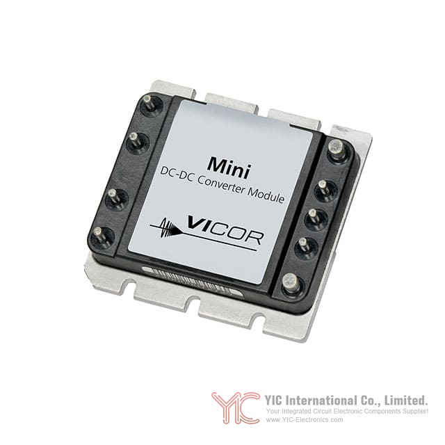
The V48B24C250B employs a compact surface-mount package with dimensions of 2.28 inches by 2.20 inches and a height of 0.50 inches above the PCB. The module's low profile enables integration into space-constrained applications while maintaining adequate clearance for airflow and thermal management.
The module utilizes ModuMate pin technology, providing a standardized interface that simplifies PCB layout and enables straightforward module replacement. The pin plating options include either RoHS-compliant gold plating (minimum 30 microinches) over a nickel barrier, or palladium (minimum 35 microinches) followed by 3 to 5 microinches of gold. Non-RoHS versions employ tin/lead 90/10 bright plating, providing compatibility with legacy manufacturing processes.
The aluminum baseplate serves as the primary thermal interface, requiring direct contact with the PCB or a thermal interface material to enable efficient heat dissipation. Manufacturing controls ensure that the spacing between the module's label surface and the PCB ranges from direct contact to the maximum gap calculated from tolerance stack-up, preventing negative tolerance accumulation that could compromise thermal performance.
PCB mounting specifications establish the footprint and via placement requirements for optimal thermal and electrical performance. The design guide provides detailed mounting recommendations including via placement for thermal coupling, trace routing for signal integrity, and spacing requirements for component clearance.
Input and output connections require careful attention to minimize parasitic inductance and resistance. Input bypass capacitors (C1-C5 in the basic operation diagram) should be mounted with short leads and connections to minimize high-frequency impedance. The bypass capacitor network typically includes a combination of ceramic and electrolytic capacitors selected to provide low impedance across the frequency spectrum from DC to several megahertz.
Application Considerations and System Design Guidelines for the V48B24C250B
The V48B24C250B operates reliably across a broad range of application scenarios, from steady-state operation to dynamic loading conditions. However, several design considerations warrant attention to ensure optimal performance and reliability.
Dynamic loading conditions where load current changes exceed 25% of the rated 10.42A require careful analysis to ensure that the converter's transient response remains adequate. Applications subject to such dynamic loading should be reviewed by Vicor applications engineering to verify that the converter will operate properly under the specific load profile. The converter's output impedance and transient response characteristics determine how quickly the output voltage recovers following a load step, with implications for downstream circuit operation.
Under light-load, no-load, or dynamic-load conditions, the converter may emit audible noise due to the switching frequency modulation that occurs at reduced power levels. System designers should consider acoustic requirements when specifying the V48B24C250B for noise-sensitive applications, potentially implementing acoustic enclosures or frequency management strategies if necessary.
Remote-sense operation, where the sense pins connect to the load rather than the converter output terminals, may require compensation circuitry to offset phase lag caused by external output leads and load impedance. The sense lead routing becomes critical in remote-sense applications, with twisted-pair routing recommended to minimize noise pickup and reduce the impedance of the sense network.
The maximum output capacitance connected to the converter output must not exceed specified limits, as excessive capacitance can compromise stability and transient response. The design guide provides detailed maximum output capacitance specifications for various operating conditions, enabling designers to select appropriate output filtering without compromising converter performance.
Applications drawing more than the rated 10.42A output current require external protection through fast-acting electronic circuit breakers. The converter's current limit provides inherent protection against sustained overcurrent, but does not tolerate intentional operation beyond rated current. Testing of current limit or short-circuit current will damage the converter, making external protection essential for applications where overcurrent risk exists.
The V48B24C250B achieves RoHS compliance when specified with F or G pin options, enabling use in applications subject to RoHS directives. The compliance status should be verified during component selection to ensure compatibility with environmental regulations applicable to the end application.
Conclusion
The V48B24C250B represents a mature, high-performance isolated DC-DC converter module that combines advanced power processing technology with flexible control architecture to address diverse application requirements. The module's 250W power delivery capability, wide 36V to 75V input range, and compact form factor establish it as a versatile solution for distributed power systems in medical, aerospace, communications, and defense applications. The integration of programmable output voltage, parallel operation capability with N+M redundancy, and comprehensive fault monitoring enables system designers to implement sophisticated power architectures without requiring extensive external support circuitry. Proper attention to thermal management, output filtering, and sense lead routing ensures reliable operation across the full range of specified operating conditions.
Frequently Asked Questions (FAQ)
- Q1. What input voltage range does the V48B24C250B support, and how does this compare to standard 48V bus systems?
-
- A1. The V48B24C250B accepts input voltages from 36V to 75V, providing substantial margin around the nominal 48V bus voltage. This wide range accommodates voltage drops due to cable resistance in distributed power architectures, transient overvoltages from load switching, and variations in source regulation. For example, a 48V source with ±10% regulation tolerance would produce voltages between 43.2V and 52.8V, well within the converter's operating range. The 100V surge withstand capability for 100ms further protects against transient overvoltages that might occur during system switching events.
- Q2. How does the V48B24C250B's efficiency rating of up to 90% impact thermal design and system power consumption?
-
- A2. The 90% efficiency rating means that for every 250W delivered to the output, approximately 28W is dissipated as heat within the converter. This thermal load must be managed through proper baseplate coupling to a heat sink or PCB thermal plane. In a system delivering 250W continuously, the 28W internal dissipation represents approximately 10% of the total system power, a manageable figure when thermal design follows recommended practices. Lower efficiency at reduced load levels means that light-load operation generates proportionally less heat, simplifying thermal management in applications with variable power demands.
- Q3. Can multiple V48B24C250B modules be paralleled for higher power delivery, and what redundancy benefits does this provide?
-
- A3. Yes, multiple V48B24C250B modules can be paralleled through the PR pin interface to deliver combined power with N+1 or N+M redundancy. For example, three modules can be paralleled using AC-coupled single-wire interface to deliver 750W total power while maintaining operation if any single module fails. Four or more modules require transformer-coupled interface architecture. The redundancy benefit means that if one module fails, the remaining modules continue to supply power to the load at reduced capacity, enabling graceful degradation rather than complete system failure. This architecture proves valuable in applications where power continuity is essential.
- Q4. What is the significance of the ±0.2% output regulation specification, and how does it affect downstream circuit design?
-
- A4. The ±0.2% regulation specification means that the 24V output will remain between 23.952V and 24.048V from no-load to full-load operation. This tight regulation eliminates the need for additional voltage regulation stages in many applications, simplifying circuit design and reducing component count. For analog circuits requiring stable reference voltages, this regulation performance proves sufficient for direct connection without additional buffering. Digital circuits benefit from the stable supply voltage, reducing noise margins and improving signal integrity. Applications with more stringent voltage stability requirements can implement local linear regulators powered by the V48B24C250B output, leveraging the converter's stable baseline to achieve even tighter regulation if needed.
- Q5. How does the output voltage programming capability of the V48B24C250B enable system optimization?
-
- A5. The V48B24C250B supports output voltage adjustment from 90% to 110% of nominal (21.6V to 26.4V for the 24V model) through resistor or potentiometer connection to the SC pin. This programmability enables several optimization strategies: voltage can be reduced to minimize power dissipation in loads during light-load operation, increased to compensate for voltage drops in long distribution networks, or adjusted dynamically in response to changing system conditions. For example, a system with 1 meter of output cabling might experience 0.5V drop at full load, requiring the converter output to be trimmed up by approximately 2% to maintain 24V at the load. The online trim calculators simplify the process of determining appropriate resistor values for specific trim percentages.
- Q6. What protection mechanisms does the V48B24C250B incorporate, and what external protection is required?
-
- A6. The V48B24C250B incorporates internal watchdog circuitry that monitors input voltage, operating temperature, and internal operating parameters, automatically shutting down if any parameter exceeds safe limits. The module also includes current limiting that prevents sustained overcurrent operation. However, the converter does not tolerate intentional operation beyond rated current, and testing of current limit or short-circuit current will damage the module. Applications where overcurrent risk exists require external fast-acting electronic circuit breakers to protect the converter. The input surge withstand capability of 100V for 100ms provides protection against transient overvoltages without requiring external protection in most applications.
- Q7. How should the V48B24C250B be stored to maintain long-term reliability?
-
- A7. The V48B24C250B should be stored in ESD-safe packaging in accordance with ANSI/ESD S20.20 standards when not installed in customer units. Storage environment should be temperature-controlled between 15°C and 38°C with non-condensing humidity and no minimum humidity requirement when stored in ESD-compliant packaging. These storage conditions prevent moisture absorption, thermal stress, and electrostatic damage that could compromise module reliability. Modules stored outside these conditions may experience degraded performance or premature failure when subsequently installed in applications.
- Q8. What role does the PC pin play in system-level control, and how can it be utilized for status indication?
-
- A8. The PC pin serves dual functions: it enables system-level enable/disable control by pulling the pin low (maximum 2.3V) to disable the converter, and it provides an auxiliary power source during normal operation capable of sourcing 5.7V at 1.5mA. This auxiliary output can power status indication circuits such as LEDs that signal converter operational status without requiring a separate power supply. The PC pin also transitions low during fault conditions detected by the watchdog circuitry, providing a system-level indication that the converter has shut down due to an out-of-specification condition. The limited current capacity (1.5mA) requires careful load design to avoid exceeding the available power budget.
- Q9. What thermal considerations are important for reliable V48B24C250B operation at maximum power?
-
- A9. The V48B24C250B maintains full 250W output power up to a baseplate temperature of 100°C. Reliable operation requires that the baseplate temperature remain below this limit under the worst-case combination of ambient temperature and thermal load. The module's thermal resistance from junction to baseplate, combined with the system's thermal resistance from baseplate to ambient, determines the junction temperature rise above ambient. For example, if the module dissipates 28W (at 90% efficiency) and the thermal resistance from baseplate to ambient is 2°C/W, the baseplate temperature will rise 56°C above ambient. In a 50°C ambient environment, the baseplate would reach 106°C, exceeding the 100°C limit. This scenario would require either improved thermal coupling (lower thermal resistance) or reduced power delivery to maintain safe operation.
- Q10. How does the isolated output architecture of the V48B24C250B benefit system design compared to non-isolated converters?
-
- A10. The 1500V DC isolation between input and output eliminates ground loops that can cause noise coupling in multi-voltage systems. This isolation proves particularly valuable in applications where the input and output circuits operate at different ground potentials or where multiple converters supply different voltage rails. The isolation also provides protection against transient events that might otherwise couple noise into sensitive circuits. For example, in a system with both 48V and 24V rails, the isolation prevents 48V transients from coupling into the 24V output through parasitic capacitance paths. This isolation capability simplifies system design by reducing the need for external isolation transformers or opto-isolators in many applications.