Understanding Multilayer Ceramic Capacitor Technology and the CL31C330JIFNFNE Design
Multilayer ceramic capacitors function by stacking alternating layers of ceramic dielectric material and metallic electrodes. Each layer contributes to the overall capacitance, allowing manufacturers to achieve precise capacitance values in compact packages. The CL31C330JIFNFNE employs this stacking principle to deliver 33 pF of capacitance within its 1206 form factor.
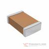
The ceramic body of the CL31C330JIFNFNE serves as the dielectric medium, positioned between internal electrodes that accumulate and release electrical charge. The nickel plating on the ceramic body provides a barrier against environmental degradation, while the tin-plated terminations facilitate reliable solder connections during PCB assembly. This construction methodology ensures that the CL31C330JIFNFNE maintains stable electrical performance throughout its operational lifetime.
The internal electrode structure of the CL31C330JIFNFNE is engineered to minimize parasitic inductance and resistance, characteristics that become increasingly important at higher frequencies and voltages. The use of copper in limited internal electrode applications further optimizes the electrical path, reducing losses and improving overall device efficiency.
Decoding the CL31C330JIFNFNE Part Number System
The part number CL31C330JIFNFNE follows Samsung Electro-Mechanics' standardized nomenclature, with each character position conveying specific technical information about the CL31C330JIFNFNE variant.
The prefix "CL" identifies this component as a multilayer ceramic capacitor. The subsequent digits and letters encode the physical size, dielectric material, capacitance value, tolerance, voltage rating, thickness, termination specifications, and packaging format. For the CL31C330JIFNFNE specifically, the "31" indicates the 1206 package size, while "C" denotes the COG/NP0 dielectric classification. The "330" represents the capacitance value of 33 pF (expressed as 33 followed by one zero). The "J" tolerance code indicates ±5% accuracy, and the "I" voltage code specifies the 1000V rating.
Understanding this nomenclature system allows design engineers to quickly identify alternative CL31C330JIFNFNE variants or related products within Samsung Electro-Mechanics' portfolio. The systematic approach to part numbering reduces confusion during component selection and procurement processes.
Electrical Specifications and Performance Characteristics of the CL31C330JIFNFNE
The CL31C330JIFNFNE operates within well-defined electrical parameters that govern its suitability for specific circuit applications. At its rated voltage of 1000V, the device maintains stable capacitance across the specified frequency range. The ±5% tolerance ensures that individual units fall within a predictable capacitance window, enabling circuit designers to account for component variation in their calculations.
Capacitance measurement of the CL31C330JIFNFNE should follow standardized conditions: measurement at 1 kHz frequency with 1.0V AC signal for Class I devices. This standardization ensures consistency across manufacturing batches and allows meaningful comparison with published specifications. The dissipation factor (DF) of the CL31C330JIFNFNE remains low, reflecting the minimal energy loss inherent to Class I ceramic dielectrics.
Insulation resistance of the CL31C330JIFNFNE exceeds specified minimums when measured one minute after applying rated DC voltage. This characteristic indicates the device's ability to maintain electrical isolation between its internal electrodes and external environment, a critical parameter for high-voltage applications where leakage current must remain negligible.
The impedance characteristics of the CL31C330JIFNFNE vary with frequency, exhibiting capacitive behavior at low frequencies and inductive behavior at higher frequencies. The self-resonant frequency (SRF) represents the point where capacitive and inductive reactances cancel, leaving only resistance. Understanding these frequency-dependent characteristics allows engineers to predict the CL31C330JIFNFNE's performance in actual circuit implementations.
Dielectric Material Options and Temperature Stability in the CL31C330JIFNFNE Series
The CL31C330JIFNFNE employs COG/NP0 dielectric material, a Class I ceramic formulation that provides exceptional temperature stability. The COG designation indicates that the capacitance change across the operating temperature range remains minimal, typically within ±30 ppm per degree Celsius. This stability makes the CL31C330JIFNFNE suitable for precision circuits where temperature-induced capacitance drift could compromise performance.
Class I dielectrics like those used in the CL31C330JIFNFNE exhibit linear voltage-capacitance relationships, meaning capacitance remains essentially constant regardless of applied voltage. This linearity contrasts sharply with Class II dielectrics, which show significant capacitance variation with voltage. For applications requiring predictable, stable capacitance values, the CL31C330JIFNFNE's Class I characteristics provide distinct advantages.
The temperature coefficient of capacitance (TCC) for the CL31C330JIFNFNE remains within tight bounds across the full operating temperature range. This predictability allows circuit designers to calculate temperature-induced performance variations with confidence, enabling compensation strategies when necessary. The CL31C330JIFNFNE maintains its specified capacitance value from -55°C to +125°C, covering the temperature extremes encountered in most industrial and commercial applications.
Reliability Levels: Standard, High Level I, and High Level II Variants of the CL31C330JIFNFNE
Samsung Electro-Mechanics offers the CL31C330JIFNFNE in three distinct reliability classifications, each addressing different application requirements and environmental demands.
The Standard variant of the CL31C330JIFNFNE represents the baseline offering, suitable for consumer electronics and general-purpose applications. This version undergoes standard reliability testing but does not incorporate enhanced moisture resistance or mechanical stress tolerance. Standard CL31C330JIFNFNE units perform reliably in controlled indoor environments where temperature and humidity remain relatively stable.
High Level I CL31C330JIFNFNE variants incorporate improved reliability features targeting industrial applications. These units undergo enhanced moisture resistance testing at 65°C and 90% relative humidity for 500 hours, demonstrating superior performance in humid environments. The High Level I CL31C330JIFNFNE also features reinforced bending strength evaluation during outgoing inspection, ensuring the device can withstand mechanical stresses encountered during PCB assembly and field deployment.
High Level II CL31C330JIFNFNE variants represent the premium reliability tier, designed for outdoor industrial applications and environments with extreme temperature and humidity fluctuations. These units undergo reinforced reliability testing at 85°C and 85% relative humidity for 1000 hours, demonstrating exceptional moisture resistance. The High Level II CL31C330JIFNFNE exhibits superior bending strength characteristics, with some variants rated for 3mm board deflection compared to the standard 2mm specification.
Selection between Standard, High Level I, and High Level II CL31C330JIFNFNE variants depends on the specific application environment. Consumer devices typically employ Standard variants, while industrial equipment and outdoor installations benefit from High Level I or High Level II specifications.
Specialized Variants of the CL31C330JIFNFNE: Enhanced Performance Solutions
Beyond the standard reliability classifications, Samsung Electro-Mechanics offers specialized CL31C330JIFNFNE variants addressing specific performance requirements.
High Bending Strength CL31C330JIFNFNE variants incorporate soft termination technology that absorbs mechanical stress caused by PCB flexing. The metal-epoxy termination construction allows the device to accommodate board deflection without cracking, making these variants ideal for applications involving flexible substrates or high-stress mounting locations. The soft termination approach represents a significant advancement over rigid termination designs, particularly for compact devices where space constraints force tight component placement.
Low Acoustic Noise CL31C330JIFNFNE variants address the piezoelectric phenomenon inherent to ceramic capacitors. When subjected to AC or pulse voltages, ceramic dielectrics can vibrate at audible frequencies, generating noise that propagates through the PCB to the system enclosure. Low Acoustic Noise variants employ specialized construction techniques to suppress these vibrations, reducing audible noise by measurable amounts. This capability proves valuable in audio equipment, precision measurement instruments, and other applications where acoustic performance matters.
Low ESL (Equivalent Series Inductance) CL31C330JIFNFNE variants minimize parasitic inductance through innovative electrode configurations. These designs employ multiple internal terminals or reverse-mounted configurations that reduce the current path length, lowering ESL values significantly. Low ESL variants enable faster energy transfer to high-speed integrated circuits, improving power delivery network performance in demanding applications.
Land Side Capacitor (LSC) variants of the CL31C330JIFNFNE mount between solder balls on high-density interconnect substrates, reducing module thickness and improving current delivery to high-speed processors. These specialized variants find application in mobile devices, wearable electronics, and compact computing modules where space optimization is paramount.
Packaging and Supply Chain Considerations for the CL31C330JIFNFNE
The CL31C330JIFNFNE ships in standardized packaging formats designed to facilitate automated assembly while protecting components during storage and transportation. Cardboard tape with 4mm pitch represents the standard packaging option, accommodating the component in embossed plastic carriers that prevent movement during handling. Alternative packaging includes 1mm and 2mm pitch options for high-density applications requiring tighter component spacing.
Reel sizes for the CL31C330JIFNFNE follow industry standards, with 7-inch and 13-inch reels available depending on order quantities. Each reel includes comprehensive labeling indicating chip size, temperature characteristics, nominal capacitance, model name, lot number, and quantity. This labeling system enables traceability throughout the supply chain, supporting quality assurance and failure analysis efforts.
Box packaging for the CL31C330JIFNFNE employs double-wall construction with inner and outer boxes, protecting components during transportation by vehicle, aircraft, or ship. The packaging design minimizes deformation risk while maintaining environmental protection. Moisture sensitivity level (MSL) rating of 1 indicates unlimited shelf life under normal storage conditions, eliminating concerns about moisture absorption during extended warehousing.
The CL31C330JIFNFNE maintains RoHS3 compliance and REACH compliance status, meeting environmental regulations in major markets. ECCN classification as EAR99 indicates the component faces no export restrictions, facilitating global supply chain operations. These regulatory alignments ensure the CL31C330JIFNFNE can be freely sourced and deployed across international markets.
Application Domains for the CL31C330JIFNFNE
The CL31C330JIFNFNE finds application across diverse electronic systems where high-voltage stability and precision capacitance prove necessary.
In smartphone and tablet applications, the CL31C330JIFNFNE serves in power management circuits, filtering high-frequency noise from voltage regulators and charging systems. The compact 1206 package accommodates space-constrained designs while the high voltage rating provides margin for transient overvoltages. Multiple CL31C330JIFNFNE units often work in parallel to achieve the aggregate capacitance required for effective power supply decoupling.
Laptop and personal computer designs employ the CL31C330JIFNFNE in memory subsystems, storage interfaces, and wireless connectivity modules. The device's temperature stability ensures consistent performance across the wide thermal range encountered in portable computing, from cold startup conditions to sustained high-performance operation. The high voltage rating accommodates the elevated supply voltages used in modern processor power delivery networks.
Server and data center applications utilize the CL31C330JIFNFNE in CPU power delivery networks, where the device's low dissipation factor and stable capacitance support efficient power conversion. High-reliability variants ensure long service life in always-on computing environments where component failures directly impact system availability and revenue generation.
Network base station equipment employs the CL31C330JIFNFNE in RF power amplifier circuits and signal processing modules. The device's high voltage rating and low acoustic noise characteristics prove valuable in these demanding applications where signal integrity and reliability determine network performance.
DC-DC converter applications across all these domains benefit from the CL31C330JIFNFNE's stable capacitance and low ESR characteristics. The device effectively filters converter output ripple while maintaining efficiency through minimal energy dissipation.
Critical Design and Integration Guidelines for the CL31C330JIFNFNE
Successful implementation of the CL31C330JIFNFNE requires careful attention to design and assembly practices that protect the component from mechanical and thermal stress.
PCB layout considerations for the CL31C330JIFNFNE include positioning the device away from board edges and cutouts where mechanical stress concentrates. Mounting the CL31C330JIFNFNE with its major axis parallel to the direction of applied stress reduces the likelihood of cracking during board flexing. Avoiding placement near screw holes minimizes exposure to board deflection caused by fastener torque.
Reflow soldering of the CL31C330JIFNFNE requires careful temperature profile management. Peak reflow temperature should not exceed 260°C, with the component spending minimal time above 240°C. Preheating all PCB constituents before reflow reduces thermal shock to the CL31C330JIFNFNE, preventing cracking caused by rapid temperature transitions. The number of reflow cycles should not exceed three, as repeated thermal cycling accelerates degradation of solder joints and internal connections.
Solder paste application for the CL31C330JIFNFNE demands precision to ensure adequate wetting without excessive fillet height. Excessive solder creates mechanical stress during cooling, while insufficient solder results in weak adhesion and potential component detachment. Proper land pattern design, following industry guidelines for the 1206 package, ensures optimal solder distribution.
Manual soldering of the CL31C330JIFNFNE should be avoided when possible, as the high temperatures and localized heating create significant cracking risk. When manual soldering becomes necessary, preheating the PCB and component to 150-180°C before applying the soldering iron minimizes thermal shock. Contact time between the soldering iron and component termination should not exceed 3-5 seconds.
Post-assembly handling of PCBs populated with the CL31C330JIFNFNE requires careful support to prevent board flexing. Holding the board with both hands, supporting it near the component, prevents bending that could crack the device. Dropped boards should be discarded rather than deployed, as internal cracks may not be immediately apparent but will cause premature failure in service.
Cleaning of assembled boards containing the CL31C330JIFNFNE should employ gentle methods avoiding ultrasonic vibration that could crack the component. When ultrasonic cleaning becomes necessary, power levels should be minimized and cleaning time kept brief. High-pressure cleaning equipment requires validation before use to ensure the CL31C330JIFNFNE can withstand the mechanical forces involved.
Storage, Transportation, and Lifecycle Management of the CL31C330JIFNFNE
Proper storage conditions preserve the CL31C330JIFNFNE's solderability and electrical characteristics throughout its shelf life. Temperature should remain between 0°C and 40°C, with relative humidity maintained between 0% and 70%. Humidity above 70% accelerates oxidation of the tin-plated terminations, degrading solderability. Temperature fluctuations should be minimized to prevent condensation that could introduce moisture into the packaging.
The CL31C330JIFNFNE maintains full solderability for six months from the manufacturing date under recommended storage conditions. Components stored beyond six months should have their solderability verified before use, as oxidation may have compromised the solder joint quality. Reflow treatment at 150°C for one hour can restore solderability to aged components, though this process should be validated for specific applications.
Transportation of the CL31C330JIFNFNE requires protection from excessive temperature, humidity, and mechanical shock. Cartons should remain undamaged, and inner packaging should be protected from external forces. Vibration during transport should be minimized, as excessive mechanical shock can crack the ceramic body despite the protective packaging.
In-service operation of the CL31C330JIFNFNE demands attention to environmental conditions and electrical stresses. The device should not be exposed to corrosive gases such as hydrogen sulfide, sulfur dioxide, or chlorine, which can corrode the plating layers and degrade performance. Direct sunlight, ozone, and ultraviolet radiation should be avoided, as these environmental factors can degrade the ceramic material and solder joints.
Electrical overstress represents a significant threat to the CL31C330JIFNFNE's reliability. Surge voltages, electrostatic discharge, and other transient overvoltages can cause dielectric breakdown and catastrophic failure. Circuit design should incorporate protective measures such as transient voltage suppressors or fuses to limit the maximum voltage the CL31C330JIFNFNE experiences.
Conclusion
The Samsung Electro-Mechanics CL31C330JIFNFNE represents a mature, well-engineered solution for high-voltage, precision capacitance applications. Its Class I dielectric characteristics, stable temperature performance, and multiple reliability variants address the diverse requirements of modern electronic systems. Successful deployment requires careful attention to design practices, assembly procedures, and operational conditions that protect the component from mechanical and thermal stress. When properly implemented, the CL31C330JIFNFNE delivers reliable performance across consumer, industrial, and infrastructure applications.
Frequently Asked Questions (FAQ)
- Q1. What distinguishes the CL31C330JIFNFNE from other multilayer ceramic capacitors in Samsung Electro-Mechanics' portfolio?
-
- A1. The CL31C330JIFNFNE combines a specific capacitance value (33 pF), voltage rating (1000V), package size (1206), and dielectric type (COG/NP0) that addresses applications requiring high-voltage stability with minimal temperature drift. The Class I dielectric ensures capacitance remains essentially constant across temperature and voltage variations, differentiating it from Class II alternatives that exhibit significant capacitance changes under these conditions.
- Q2. How does the ±5% tolerance of the CL31C330JIFNFNE affect circuit design?
-
- A2. The ±5% tolerance means individual CL31C330JIFNFNE units may vary from 31.35 pF to 34.65 pF. Circuit designers must account for this variation when calculating filter cutoff frequencies, resonant frequencies, or other capacitance-dependent parameters. In precision applications, multiple CL31C330JIFNFNE units can be paralleled to reduce the proportional tolerance impact, or trimmer capacitors can be incorporated to fine-tune circuit performance.
- Q3. What is the significance of the 1000V rating for the CL31C330JIFNFNE?
-
- A3. The 1000V rating indicates the maximum continuous DC voltage the CL31C330JIFNFNE can safely withstand without risk of dielectric breakdown. This high voltage rating makes the device suitable for power conversion circuits, high-voltage signal conditioning, and other applications where supply voltages exceed typical logic levels. The rating provides margin for transient overvoltages that may occur during switching events or fault conditions.
- Q4. How should the CL31C330JIFNFNE be stored to maintain solderability?
-
- A4. The CL31C330JIFNFNE should be stored in sealed packaging at temperatures between 0°C and 40°C with relative humidity between 0% and 70%. The component maintains full solderability for six months from the manufacturing date under these conditions. Storage in dry environments with low humidity preserves the tin-plated terminations, ensuring reliable solder wetting during assembly. Components stored beyond six months should have solderability verified before use.
- Q5. What mechanical stresses can damage the CL31C330JIFNFNE during assembly?
-
- A5. The CL31C330JIFNFNE can crack due to excessive mounting head pressure (above 300 grams-force), rapid thermal cycling during reflow soldering, board flexing during or after assembly, and mechanical shock from dropping or impact. Careful control of pick-and-place machine pressure, gradual temperature ramping during reflow, proper PCB support during assembly, and gentle handling throughout the manufacturing process minimize cracking risk.
- Q6. How does the COG/NP0 dielectric classification affect the CL31C330JIFNFNE's performance?
-
- A6. COG/NP0 classification indicates the CL31C330JIFNFNE exhibits minimal capacitance change across temperature variations, typically within ±30 ppm per degree Celsius. This stability makes the device suitable for precision circuits where temperature-induced capacitance drift could compromise performance. Unlike Class II dielectrics that show significant capacitance variation with temperature and voltage, the CL31C330JIFNFNE maintains predictable, stable capacitance values across its operating range.
- Q7. What are the differences between Standard, High Level I, and High Level II CL31C330JIFNFNE variants?
-
- A7. Standard CL31C330JIFNFNE variants suit consumer electronics in controlled environments. High Level I variants undergo enhanced moisture resistance testing (65°C, 90% RH, 500 hours) and reinforced bending strength evaluation, making them suitable for industrial applications. High Level II variants undergo more stringent testing (85°C, 85% RH, 1000 hours) and offer superior bending strength, making them appropriate for outdoor industrial installations and extreme environments.
- Q8. Can the CL31C330JIFNFNE be used in AC voltage applications?
-
- A8. Yes, the CL31C330JIFNFNE can be used in AC voltage applications, provided the peak-to-peak AC voltage does not exceed the 1000V rating. However, AC current flowing through the device generates self-heating due to its equivalent series resistance (ESR). The surface temperature of the CL31C330JIFNFNE must remain within the maximum operating temperature limit, and the temperature rise from self-heating should not exceed 20°C. Circuit designers must verify these conditions are met in actual applications.
- Q9. What is the self-resonant frequency (SRF) of the CL31C330JIFNFNE, and why does it matter?
-
- A9. The SRF represents the frequency where the CL31C330JIFNFNE's capacitive reactance and inductive reactance cancel, leaving only resistance. At frequencies below SRF, the device behaves as a capacitor; above SRF, it behaves as an inductor. Understanding the SRF helps engineers predict the CL31C330JIFNFNE's impedance characteristics at different frequencies and select appropriate devices for specific circuit applications. The SRF varies with package size and internal construction, with the 1206 package typically exhibiting SRF in the megahertz range.
- Q10. How does capacitance aging affect the CL31C330JIFNFNE over time?
-
- A10. Class I dielectrics like those in the CL31C330JIFNFNE exhibit minimal aging compared to Class II alternatives. Any capacitance decrease occurs very slowly and is typically negligible for most applications. Heat treatment at 150°C for one hour can recover any aged capacitance, resetting the aging clock. For applications requiring absolute capacitance stability over extended periods, the CL31C330JIFNFNE's Class I characteristics provide significant advantages over Class II alternatives.
- Q11. What precautions should be taken when manually soldering the CL31C330JIFNFNE?
-
- A11. Manual soldering of the CL31C330JIFNFNE should be avoided when possible due to high cracking risk. When necessary, preheat the PCB and component to 150-180°C before applying the soldering iron. Use a soldering iron tip temperature of 350°C maximum, keeping contact time with the component termination below 3-5 seconds. Allow natural cooling after soldering rather than forced cooling. For components with metal-epoxy terminations, limit iron tip temperature to 300°C maximum to avoid damaging the epoxy material.
- Q12. How should the CL31C330JIFNFNE be positioned on the PCB to minimize mechanical stress?
-
- A12. Position the CL31C330JIFNFNE with its major axis parallel to the direction of applied stress to distribute mechanical loads more evenly. Avoid mounting near board edges, cutouts, or screw holes where stress concentrates. When mounting near board edges, orient the device to minimize stress concentration. Support the PCB adequately during assembly and testing to prevent flexing that could crack the component. These positioning strategies significantly reduce the likelihood of mechanical failure during assembly and field operation.
- Q13. What is the significance of the RoHS3 and REACH compliance status of the CL31C330JIFNFNE?
-
- A13. RoHS3 compliance indicates the CL31C330JIFNFNE contains no restricted hazardous substances such as lead, cadmium, or hexavalent chromium, meeting environmental regulations in the European Union and other major markets. REACH compliance indicates the component meets chemical safety requirements. These certifications ensure the CL31C330JIFNFNE can be freely sourced and deployed in regulated markets without environmental or legal concerns, simplifying global supply chain operations.
- Q14. How does the Low ESL variant of the CL31C330JIFNFNE differ from the standard version?
-
- A14. Low ESL variants minimize equivalent series inductance through specialized electrode configurations that reduce the current path length. These variants enable faster energy transfer to high-speed integrated circuits, improving power delivery network performance in demanding applications. Low ESL variants prove particularly valuable in high-frequency switching circuits and applications requiring rapid current delivery to processors or other high-speed components.
- Q15. What environmental factors can degrade the CL31C330JIFNFNE's performance during operation?
-
- A15. Corrosive gases such as hydrogen sulfide, sulfur dioxide, chlorine, and ammonia can corrode the plating layers and degrade performance. Direct sunlight, ozone, and ultraviolet radiation can damage the ceramic material and solder joints. High humidity environments can promote corrosion and moisture ingress. Vibration exceeding specified limits can cause mechanical damage. Exposure to water, oil, or conductive liquids can cause electrical failures. Proper environmental control and protective measures ensure the CL31C330JIFNFNE maintains reliable performance throughout its operational life.