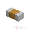
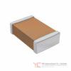
Product Overview of the Samsung CL10A106KP8NNNC Ceramic Capacitor
The Samsung CL10A106KP8NNNC is a multilayer ceramic capacitor (MLCC) designed for general-purpose applications requiring stable capacitance performance across a wide operating range. With a nominal capacitance of 10 microfarads, rated voltage of 10 volts, and X5R temperature characteristic, this component delivers reliable energy storage and filtering capabilities in compact surface-mount form factor. The 0603 package (1608 metric) provides a balance between miniaturization and handling ease, making it suitable for modern high-density circuit board designs.
The X5R dielectric material ensures that capacitance variation remains within acceptable limits across the operating temperature range of -55°C to +85°C, with a tolerance of ±10%. This temperature stability makes the CL10A106KP8NNNC particularly valuable in applications where thermal fluctuations could otherwise compromise circuit performance. The device is manufactured using Samsung Electro-Mechanics' established multilayer ceramic technology, which combines multiple ceramic layers with internal electrodes to achieve the specified capacitance in a minimal footprint.
Structural Specifications and Physical Characteristics of the CL10A106KP8NNNC
The CL10A106KP8NNNC measures 1.6 mm in length, 0.8 mm in width, and 0.8 mm in height, conforming to the 0603 package standard. This compact geometry allows for high-density placement on printed circuit boards while maintaining sufficient mechanical robustness for automated assembly processes. The component features nickel-barrier terminations with tin plating, providing excellent solderability and corrosion resistance during storage and assembly operations.
The internal structure consists of multiple ceramic dielectric layers alternated with palladium-silver internal electrodes. This multilayer construction enables the achievement of high capacitance values within the small physical envelope. The ceramic material composition and layer thickness are precisely controlled during manufacturing to ensure consistent electrical performance across production batches.
The typical weight of the CL10A106KP8NNNC is approximately 0.015 grams, contributing minimal mass to the overall assembly. The component is supplied in tape-and-reel format with either 4mm or 2mm pitch cardboard tape, or embossed plastic tape, depending on customer requirements. Standard reel sizes accommodate various production volumes, from prototype quantities to high-volume manufacturing runs.
Electrical Performance Parameters of the CL10A106KP8NNNC
The CL10A106KP8NNNC delivers 10 microfarads of capacitance at the specified measurement conditions, with a tolerance band of ±10%. This tolerance range accommodates manufacturing process variations while maintaining circuit functionality. The rated voltage of 10 volts represents the maximum continuous DC voltage that should be applied across the component terminals under normal operating conditions.
The insulation resistance of the CL10A106KP8NNNC exceeds 10,000 megohm-microfarads, measured one minute after applying the rated voltage. This high insulation resistance indicates minimal leakage current, typically in the picoampere range at room temperature. The low leakage current characteristic makes the CL10A106KP8NNNC suitable for applications requiring long-term charge retention, such as timing circuits and backup power systems.
The dissipation factor (DF) of the CL10A106KP8NNNC remains below 5% at 1 kHz and 1 volt, indicating relatively low energy loss within the dielectric material. This low loss characteristic reduces self-heating effects and improves overall circuit efficiency, particularly in applications involving AC or ripple current operation.
Capacitance Measurement and Stability Characteristics of the CL10A106KP8NNNC
Accurate capacitance measurement of the CL10A106KP8NNNC requires adherence to specific voltage and frequency conditions. For this 10-microfarad device, measurements should be performed at 1 volt AC and 1 kHz frequency, following a heat treatment cycle of 150°C for one hour with subsequent room temperature stabilization for 24 hours. These standardized conditions ensure reproducible results across different measurement facilities and enable meaningful comparison with published specifications.
When measuring capacitance, it is recommended to use impedance measurement equipment equipped with Auto Level Control (ALC) functionality. The ALC feature maintains consistent output voltage across the measurement frequency range, compensating for impedance variations that could otherwise reduce the measurement signal. Without ALC, high-capacitance devices may produce measurement errors due to excessive current draw from the measurement source.
The capacitance value of the CL10A106KP8NNNC exhibits sensitivity to both applied voltage and temperature. These dependencies must be considered during circuit design to ensure that the actual capacitance under operating conditions remains within acceptable tolerance limits. For example, when DC bias voltage is applied to the capacitor, the effective capacitance decreases from its nominal value. Similarly, temperature variations cause capacitance shifts that follow the X5R characteristic curve.
Dissipation Factor and Quality Factor in the CL10A106KP8NNNC
The dissipation factor (DF) of the CL10A106KP8NNNC represents the ratio of energy lost to energy stored within the dielectric material during each AC cycle. This loss manifests as heat generation and represents the combined effect of dielectric loss and electrode resistance. For the CL10A106KP8NNNC, the DF specification of approximately 5% at 1 kHz indicates that approximately 5% of the stored energy is dissipated as heat during each oscillation cycle.
The quality factor (Q), defined as the reciprocal of dissipation factor, provides an alternative perspective on component losses. For the CL10A106KP8NNNC with a DF of 5%, the corresponding Q factor is approximately 20. This moderate Q value reflects the inherent characteristics of Class II ceramic dielectrics, which prioritize high capacitance density over extremely low losses.
The dissipation factor of the CL10A106KP8NNNC increases with frequency and temperature. At elevated temperatures or higher frequencies, the DF may increase by 50% or more compared to the reference condition. This frequency and temperature dependence must be considered in applications involving high-frequency AC signals or operation at elevated ambient temperatures.
Insulation Resistance and Leakage Current Behavior of the CL10A106KP8NNNC
The insulation resistance of the CL10A106KP8NNNC is specified as a minimum of 10,000 megohm-microfarads, which translates to approximately 1,000 megohms for the 10-microfarad device. This high insulation resistance indicates that leakage current remains extremely low, typically in the range of 10 nanoamperes or less at room temperature and rated voltage.
Leakage current in the CL10A106KP8NNNC exhibits strong temperature dependence. As temperature increases, the leakage current approximately doubles for every 10°C rise. At the maximum operating temperature of 85°C, leakage current may increase to several hundred nanoamperes, representing a significant increase from room temperature values. This temperature-dependent leakage must be considered in applications requiring precise charge retention over extended periods at elevated temperatures.
The measurement of insulation resistance should be performed one minute after applying the rated voltage, allowing the charging current to decay and the insulation resistance to stabilize. Measurements taken immediately after voltage application will yield artificially low resistance values due to the presence of charging current superimposed on the leakage current.
Capacitance Aging Effects in the CL10A106KP8NNNC
The CL10A106KP8NNNC exhibits capacitance aging, a characteristic of Class II ceramic dielectrics where capacitance gradually decreases over time. This aging process follows a logarithmic relationship with time, meaning that the rate of capacitance decrease slows as time progresses. Immediately after manufacturing, the CL10A106KP8NNNC may experience a capacitance reduction of approximately 2-3% during the first year of storage or operation.
The aging rate of the CL10A106KP8NNNC is influenced by temperature and applied voltage. Higher temperatures and higher DC bias voltages accelerate the aging process. For applications requiring precise capacitance values over extended periods, the aging characteristic must be incorporated into circuit design calculations to ensure that the minimum capacitance limit is not violated during the product lifetime.
Heat treatment at 150°C for one hour effectively resets the aging clock of the CL10A106KP8NNNC. After such thermal treatment, the capacitance recovers partially, and the aging process recommences from this new baseline. This recovery characteristic is exploited during manufacturing quality control procedures and can be utilized in field applications if capacitance restoration is required.
Temperature Characteristics and Thermal Performance of the CL10A106KP8NNNC
The X5R temperature characteristic of the CL10A106KP8NNNC specifies that capacitance variation remains within ±15% across the operating temperature range of -55°C to +85°C. This relatively tight tolerance band makes the CL10A106KP8NNNC suitable for applications where temperature-induced capacitance shifts could compromise circuit performance. The capacitance variation follows a smooth curve with minimum capacitance typically occurring near the lower temperature extreme and maximum capacitance near room temperature.
The temperature coefficient of capacitance (TCC) of the CL10A106KP8NNNC is not constant across the temperature range. Instead, the capacitance change accelerates at temperature extremes, particularly at the lower temperature limit. This nonlinear behavior must be considered when designing circuits that operate across the full temperature range.
When DC bias voltage is applied to the CL10A106KP8NNNC, the temperature characteristics become more pronounced. The bias temperature coefficient (Bias TCC) describes how the capacitance change with temperature is modified by the presence of DC voltage. At maximum rated voltage, the Bias TCC may increase the temperature-induced capacitance variation by an additional 5-10%, requiring careful consideration in precision circuit designs.
Self-Heating and Thermal Management in the CL10A106KP8NNNC
When AC or pulse voltage is applied to the CL10A106KP8NNNC, current flowing through the equivalent series resistance (ESR) generates heat within the component. This self-heating effect can raise the surface temperature of the capacitor above the ambient temperature, potentially affecting reliability and performance. The magnitude of self-heating depends on the AC current amplitude, frequency, and the ESR value of the component.
The surface temperature of the CL10A106KP8NNNC must not exceed the maximum operating temperature of 85°C, including the effects of self-heating. Additionally, the temperature rise caused by self-heating should not exceed 20°C above the ambient temperature. These dual constraints ensure that the component operates within its design envelope and maintains long-term reliability.
For applications involving significant ripple current, such as power supply filter circuits, the self-heating effect must be calculated and verified. The ESR of the CL10A106KP8NNNC varies with frequency, typically ranging from 50 to 200 milliohms depending on the specific frequency and measurement conditions. Using the worst-case ESR value and the expected ripple current amplitude, the self-heating temperature rise can be estimated using the formula: ΔT = I²RMS × ESR / (thermal mass and dissipation characteristics).
Voltage Characteristics and DC-AC Behavior of the CL10A106KP8NNNC
The capacitance of the CL10A106KP8NNNC exhibits significant dependence on applied DC bias voltage. As DC voltage increases from zero to the rated voltage of 10 volts, the effective capacitance decreases, typically by 20-30% at full rated voltage. This DC bias characteristic reflects the nonlinear behavior of the ferroelectric ceramic dielectric material used in Class II MLCCs.
The DC bias characteristic of the CL10A106KP8NNNC must be carefully considered in circuit designs where the operating voltage approaches the rated voltage. For example, in a power supply filter circuit operating at 9 volts, the effective capacitance may be only 70-80% of the nominal 10-microfarad value, potentially affecting filter performance and ripple voltage specifications.
When AC voltage is superimposed on DC bias voltage, the CL10A106KP8NNNC exhibits additional capacitance variation. The AC voltage characteristic describes how the effective capacitance changes as the AC signal amplitude increases. This AC voltage dependence is separate from and additive to the DC bias effect, creating complex capacitance behavior in circuits with combined DC and AC signals.
The peak-to-peak AC voltage applied to the CL10A106KP8NNNC must not exceed the rated voltage of 10 volts. When DC and AC voltages are combined, the maximum instantaneous voltage (DC + peak AC) must remain below the rated voltage to prevent dielectric breakdown and ensure long-term reliability.
Impedance Analysis and Frequency Response of the CL10A106KP8NNNC
The electrical impedance of the CL10A106KP8NNNC varies significantly with frequency, following a characteristic curve that reflects the capacitive, resistive, and inductive properties of the component. At low frequencies, the impedance is dominated by the capacitive reactance, which decreases as frequency increases according to the relationship XC = 1/(2πfC). At these frequencies, the CL10A106KP8NNNC behaves as an ideal capacitor with impedance inversely proportional to frequency.
At intermediate frequencies, the impedance reaches a minimum value, which occurs at the self-resonant frequency (SRF) of the CL10A106KP8NNNC. At the SRF, the capacitive reactance and inductive reactance cancel each other, leaving only the equivalent series resistance (ESR) as the impedance. For the CL10A106KP8NNNC, the SRF typically occurs in the range of 50-100 MHz, depending on the specific component characteristics and mounting configuration.
At frequencies above the SRF, the impedance increases due to the inductive reactance of the component leads and internal structure. This inductive behavior becomes increasingly dominant at higher frequencies, eventually making the CL10A106KP8NNNC unsuitable for high-frequency filtering applications. The equivalent series inductance (ESL) of the CL10A106KP8NNNC is typically in the range of 0.5-1.0 nanohenries, contributing to the inductive reactance at high frequencies.
The ESR of the CL10A106KP8NNNC varies with frequency, typically decreasing from approximately 200 milliohms at 1 kHz to approximately 50 milliohms at 100 kHz, then increasing again at higher frequencies. This frequency-dependent ESR behavior reflects the complex internal structure of the multilayer ceramic capacitor and the frequency-dependent losses in the dielectric material and electrode materials.
Packaging and Supply Format Options for the CL10A106KP8NNNC
The CL10A106KP8NNNC is supplied in tape-and-reel format, the standard packaging for automated assembly operations. Two tape pitch options are available: 4mm pitch for lower-speed assembly equipment and 2mm pitch for high-speed automated placement machines. The 4mm pitch tape accommodates 5,000 components per reel, while the 2mm pitch tape accommodates 10,000 components per reel, enabling efficient high-volume production.
Embossed plastic tape is also available as an alternative to cardboard tape, offering improved moisture barrier properties and reduced risk of component damage during handling. The embossed tape format is particularly recommended for applications requiring extended storage periods or operation in high-humidity environments.
The CL10A106KP8NNNC is also available in box packaging for applications requiring smaller quantities or special handling requirements. Box packaging options include inner boxes containing individual reels and outer boxes for shipping and storage. The packaging label includes critical information such as chip size, temperature characteristics, nominal capacitance, model name, lot number, and quantity, enabling traceability and quality control throughout the supply chain.
The cover tape peel-off force for the CL10A106KP8NNNC is specified between 10 and 70 gram-force, ensuring that the tape can be reliably removed by automated equipment without damaging the components or leaving adhesive residue on the component surfaces.
Mounting and Assembly Considerations for the CL10A106KP8NNNC
The CL10A106KP8NNNC should be mounted with its major axis aligned parallel to the direction of applied mechanical stress. This orientation minimizes the bending stress experienced by the component during assembly and operation, reducing the risk of mechanical failure and capacitance degradation.
When mounting the CL10A106KP8NNNC near PCB cutouts or edges, the mechanical stress concentration must be carefully managed. The stress experienced by the component increases significantly when positioned near board edges or cutouts, with stress levels potentially doubling or tripling compared to components mounted in the board interior. Whenever possible, the CL10A106KP8NNNC should be positioned at least 5mm away from board edges and cutouts.
Similarly, when the CL10A106KP8NNNC is mounted near screw holes, the board deflection caused by screw torque can induce significant mechanical stress on the component. The component should be positioned as far as possible from screw holes, with a minimum distance of 10mm recommended to minimize stress transfer.
The mounting head pressure applied by pick-and-place equipment should not exceed 300 gram-force to prevent mechanical damage to the CL10A106KP8NNNC. Excessive pressure can cause internal cracks in the ceramic dielectric, leading to premature failure or performance degradation. Regular maintenance and calibration of mounting equipment is essential to ensure consistent pressure application.
Soldering Processes and Thermal Profile Requirements for the CL10A106KP8NNNC
The CL10A106KP8NNNC is designed for reflow soldering, the primary assembly method for surface-mount components. The recommended reflow profile specifies a peak temperature of 260°C ±5°C with a dwell time of 30 seconds at peak temperature. This thermal profile must be carefully controlled to ensure adequate solder wetting while minimizing thermal stress on the component.
The reflow process should include a preheat phase where the entire PCB and all components are gradually heated to approximately 150-180°C before the peak temperature is reached. This preheat phase is essential for minimizing thermal shock and reducing the risk of mechanical damage to the CL10A106KP8NNNC. The temperature difference between the PCB and component surface should be kept to a minimum throughout the reflow process.
The number of reflow cycles should be limited to three or fewer to minimize cumulative thermal stress on the CL10A106KP8NNNC. If additional reflow cycles are required due to rework or repair operations, the component reliability may be compromised, and special evaluation is recommended before proceeding.
Natural air cooling is recommended after the peak temperature is reached. Forced air cooling or rapid cooling methods should be avoided, as they can induce additional thermal stress and increase the risk of mechanical failure. The cooling rate should be gradual, allowing the component and PCB to cool uniformly.
Flow soldering is an alternative assembly method suitable for the CL10A106KP8NNNC, with a peak temperature limit of 260°C and a maximum dwell time of 5 seconds. Flow soldering is typically used for through-hole components but can be applied to surface-mount components in specific manufacturing scenarios. The shorter dwell time compared to reflow soldering reduces thermal stress but requires careful process control to ensure adequate solder wetting.
Mechanical Stress Management During Assembly of the CL10A106KP8NNNC
When assembling double-sided PCBs with the CL10A106KP8NNNC mounted on both sides, the component on the first side experiences significant mechanical stress during the mounting of components on the second side. The suction nozzle pressure applied to the opposite side of the board can cause board deflection, inducing bending stress on the CL10A106KP8NNNC on the first side.
To minimize this stress, the PCB should be supported from the back side during the mounting of components on the second side. Support pins or a dedicated support fixture should be positioned as close as possible to the mounting location to minimize board deflection. The support structure should be rigid enough to prevent any visible board movement during the mounting process.
The suction nozzle and mounting claw of the pick-and-place equipment should be regularly inspected and maintained. Dust accumulation in the suction mechanism or wear of the mounting claw can cause uneven force distribution during component placement, leading to mechanical damage to the CL10A106KP8NNNC. Regular cleaning and replacement of worn components is essential for maintaining consistent assembly quality.
Bending stress during manual handling of assembled PCBs must also be minimized. The PCB should always be held with both hands along the edges to prevent board flexing. Single-handed handling or holding the board by the center can cause significant bending stress, potentially damaging the CL10A106KP8NNNC and compromising long-term reliability.
Post-Assembly Handling and Reliability Protection for the CL10A106KP8NNNC
After soldering, the CL10A106KP8NNNC must be protected from mechanical shock and vibration. Dropped PCBs or boards subjected to impact can cause internal cracks in the ceramic dielectric, leading to degraded insulation resistance and potential short-circuit failures. Dropped boards should never be used in production, as the damage may not be immediately apparent but can manifest as field failures.
When testing the electrical performance of the CL10A106KP8NNNC after assembly, the PCB must be properly supported to prevent bending caused by test probe pressure. Support pins should be positioned on the back side of the PCB, as close as possible to the test probe location, to minimize board deflection. Excessive board bending during testing can cause mechanical damage to the CL10A106KP8NNNC and solder joint failures.
The CL10A106KP8NNNC should not be subjected to vibration or mechanical shock exceeding the specified limits during operation. If the application environment involves significant vibration, special vibration-resistant variants of the component should be considered. The standard CL10A106KP8NNNC is designed for typical electronic equipment environments and may not be suitable for applications involving continuous vibration or mechanical shock.
Storage, Transportation, and Environmental Requirements for the CL10A106KP8NNNC
The CL10A106KP8NNNC should be stored in a controlled environment with temperature maintained between 0°C and 40°C and relative humidity between 0% and 70%. Excessive temperature or humidity can degrade the component quality and compromise solderability. High humidity environments accelerate oxidation of the tin plating on the component terminations, reducing solder wettability and increasing the risk of assembly defects.
The shelf life of the CL10A106KP8NNNC is specified as six months from the date of manufacture. Components stored beyond this period should have their solderability verified before use. Extended storage, particularly in high-humidity environments, can result in oxidation of the termination plating, requiring additional cleaning or flux application during assembly.
During transportation, the CL10A106KP8NNNC must be protected from excessive temperature fluctuations, mechanical shock, and vibration. The packaging should be designed to absorb shock and prevent component movement within the shipping container. Temperature cycling during transportation can cause condensation on the component surfaces, potentially compromising solderability if the components are not allowed to dry before assembly.
The CL10A106KP8NNNC should not be exposed to corrosive gases such as hydrogen sulfide, sulfur dioxide, chlorine, or ammonia during storage or transportation. These gases can corrode the tin plating on the component terminations, degrading solderability and potentially causing assembly defects. Storage facilities should be located away from industrial areas with significant air pollution.
Electrical Overstress Protection and Surge Handling for the CL10A106KP8NNNC
The CL10A106KP8NNNC is susceptible to damage from electrical overstress (EOS) events, including surge voltage and electrostatic discharge (ESD). Surge voltage can cause dielectric breakdown in the CL10A106KP8NNNC, resulting in electrical short failure. The magnitude and duration of the surge voltage determine the severity of damage, with higher voltages and longer durations causing more severe damage.
Electrostatic discharge can damage the CL10A106KP8NNNC even though the charge quantity is relatively small. The high voltage associated with ESD events can exceed the dielectric breakdown strength of the ceramic material, causing permanent damage. Low-capacitance devices are particularly vulnerable to ESD damage due to their lower charge storage capacity.
During circuit design, protective measures should be implemented to limit surge voltage and ESD exposure to the CL10A106KP8NNNC. Surge protection devices such as varistors or transient voltage suppressors should be positioned to limit voltage spikes before they reach the capacitor. ESD protection should be implemented at circuit board edges and connector locations where external ESD events are most likely to occur.
The actual applied voltage to the CL10A106KP8NNNC must not exceed the rated voltage of 10 volts under any circumstances. For DC voltage or DC+AC voltage applications, the DC component or the maximum value of DC+AC should not exceed the rated voltage. For AC or pulse voltage applications, the peak-to-peak value should not exceed the rated voltage. Abnormal voltages such as surge or static electricity must also be limited to the rated voltage.
PCB Design Considerations and Land Pattern Optimization for the CL10A106KP8NNNC
The PCB land pattern for the CL10A106KP8NNNC must be carefully designed to ensure proper solder joint formation and minimize mechanical stress. The land dimensions should be optimized based on the specific soldering process (reflow or flow) and the solder paste characteristics. Oversized land patterns result in excessive solder fillet height, increasing mechanical stress on the component and the risk of cracking. Undersized land patterns result in insufficient solder volume, compromising solder joint strength and potentially causing component detachment.
The solder paste application should be uniform across the land pattern, with thickness typically between 0.1 and 0.15 mm. Excessive solder paste results in large solder fillets that concentrate stress on the component terminations. Insufficient solder paste results in weak solder joints that may fail under thermal cycling or mechanical stress.
The PCB material selection affects the mechanical stress experienced by the CL10A106KP8NNNC. The thermal expansion coefficient of the PCB should be as close as possible to that of the ceramic capacitor to minimize stress during thermal cycling. Standard glass-epoxy PCB material has a thermal expansion coefficient of approximately 16 ppm/°C in the X-Y plane, which is significantly higher than the ceramic material (approximately 5-7 ppm/°C), creating thermal stress during temperature changes.
The PCB thickness and layer stackup should be designed to minimize board deflection during assembly and operation. Thicker PCBs and proper support structures reduce board bending and the associated mechanical stress on the CL10A106KP8NNNC. For high-density boards with many components, careful placement of support structures and mounting fixtures is essential to maintain board rigidity.
System-Level Design Evaluation and Derating Guidelines for the CL10A106KP8NNNC
The actual operating conditions of the CL10A106KP8NNNC must be evaluated within the context of the complete system design. The capacitance value under actual operating conditions may differ significantly from the nominal value due to the combined effects of DC bias voltage, AC voltage, temperature, and aging. For applications requiring precise capacitance values, these effects must be calculated and incorporated into the circuit design.
Derating guidelines should be applied to ensure long-term reliability of the CL10A106KP8NNNC. The operating voltage should be limited to a percentage of the rated voltage, typically 50-80% depending on the application requirements and reliability targets. Similarly, the operating temperature should be limited to a percentage of the maximum rated temperature to provide margin for thermal transients and self-heating effects.
The surge resistance of the CL10A106KP8NNNC must be evaluated based on the actual system inductance and switching characteristics. Excessive surge voltage caused by system inductance can damage the component even if the steady-state voltage is within specifications. Circuit design should include surge protection measures such as snubber networks or transient voltage suppressors to limit surge voltage to acceptable levels.
The reliability of the CL10A106KP8NNNC is affected by the cumulative thermal stress experienced during the product lifetime. Thermal cycling between the minimum and maximum operating temperatures accelerates aging and can reduce the component lifetime. System designs should minimize thermal cycling and maintain operating temperatures as close as possible to the nominal design temperature.
Conclusion
The Samsung CL10A106KP8NNNC represents a mature, well-characterized multilayer ceramic capacitor technology suitable for a wide range of general-purpose applications. Its 10-microfarad capacitance, 10-volt rating, and X5R temperature characteristic provide stable performance across typical operating environments. Successful implementation requires careful attention to electrical characteristics including DC bias effects, temperature coefficients, and aging behavior, as well as mechanical considerations during assembly and operation. Proper PCB design, controlled soldering processes, and protection from electrical overstress ensure reliable long-term performance. The component's compact 0603 package enables high-density circuit designs while maintaining adequate mechanical robustness for automated assembly processes.
Frequently Asked Questions (FAQ)
- Q1. How does the capacitance of the CL10A106KP8NNNC change when DC voltage is applied?
-
- A1. The capacitance of the CL10A106KP8NNNC decreases as DC bias voltage increases. At the rated voltage of 10 volts, the effective capacitance may be 20-30% lower than the nominal 10-microfarad value measured at zero bias voltage. This DC bias characteristic must be considered in circuit designs where the operating voltage approaches the rated voltage, as the actual capacitance available for filtering or energy storage may be significantly less than expected.
- Q2. What is the maximum temperature rise allowed due to self-heating in the CL10A106KP8NNNC?
-
- A2. The temperature rise caused by self-heating in the CL10A106KP8NNNC must not exceed 20°C above the ambient temperature. Additionally, the total surface temperature of the component, including self-heating effects, must not exceed the maximum operating temperature of 85°C. These dual constraints ensure that the component operates within its design envelope and maintains long-term reliability in applications involving AC or ripple current.
- Q3. How should the CL10A106KP8NNNC be stored to maintain solderability?
-
- A3. The CL10A106KP8NNNC should be stored in a controlled environment with temperature between 0°C and 40°C and relative humidity between 0% and 70%. The shelf life is specified as six months from the manufacturing date. Components stored beyond six months should have their solderability verified before use, as extended storage can result in oxidation of the tin plating on the terminations, reducing solder wettability.
- Q4. What is the self-resonant frequency (SRF) of the CL10A106KP8NNNC?
-
- A4. The self-resonant frequency of the CL10A106KP8NNNC typically occurs in the range of 50-100 MHz. At the SRF, the capacitive reactance and inductive reactance cancel each other, and the impedance is determined solely by the equivalent series resistance (ESR). Above the SRF, the component exhibits inductive behavior and becomes increasingly unsuitable for high-frequency filtering applications.
- Q5. How does capacitance aging affect the long-term performance of the CL10A106KP8NNNC?
-
- A5. The CL10A106KP8NNNC exhibits capacitance aging, where the capacitance gradually decreases over time following a logarithmic relationship. Approximately 2-3% capacitance reduction may occur during the first year of operation. This aging effect must be considered in circuit designs requiring precise capacitance values over extended periods. Heat treatment at 150°C for one hour can partially recover the aged capacitance and reset the aging clock.
- Q6. What is the recommended reflow soldering profile for the CL10A106KP8NNNC?
-
- A6. The recommended reflow profile specifies a peak temperature of 260°C ±5°C with a dwell time of 30 seconds at peak temperature. A preheat phase should gradually raise the PCB and component temperature to 150-180°C before reaching peak temperature. Natural air cooling is recommended after peak temperature is reache