Product Overview of the STP16CPPS05PTR
The STP16CPPS05PTR is a monolithic, low-voltage LED driver IC designed specifically for LED panel display applications. This 16-bit constant current sink driver integrates a serial-in, parallel-out shift register architecture with 16 regulated current source outputs, enabling efficient control of LED arrays through a single serial data interface. The device operates from a 3 V to 5 V power supply, making it compatible with both legacy 5 V systems and modern 3.3 V microcontroller environments.
The STP16CPPS05PTR addresses a fundamental challenge in LED display design: the need to drive multiple LED channels with precise, adjustable current levels while minimizing power consumption and system complexity. By combining shift register functionality with constant current regulation, the device reduces the number of control lines required from a microcontroller, simplifying PCB layout and firmware implementation.
Architecture and Operating Principles of the STP16CPPS05PTR
The STP16CPPS05PTR employs a three-stage architecture that separates data input, storage, and output functions. The first stage consists of a 16-bit serial-in shift register that accepts data sequentially through a single serial data input (SDI) pin. Data is clocked into this register at rates up to 30 MHz, allowing rapid configuration updates. The second stage comprises a 16-bit D-type storage register (latch) that captures and holds the shift register contents when triggered by the latch enable (LE) signal. This separation between the shift register and storage register prevents output glitching during data entry—a critical feature in display applications where visual artifacts must be avoided.
The third stage contains 16 independent constant current source circuits. Each source is designed to deliver a regulated current to its corresponding LED output, regardless of variations in LED forward voltage or supply voltage fluctuations. This constant current approach ensures uniform LED brightness across the array and maintains consistent performance even as LEDs age or operating conditions change.
The device operates in two fundamental modes: data entry mode and output control mode. During data entry, the shift register accepts serial data while the latch holds the previous output state, allowing seamless updates without affecting display output. Once all 16 bits have been entered, the LE signal transitions to latch the new data into the storage register, updating all 16 outputs simultaneously. The output enable (OE) pin provides independent control over whether the latched data drives the output stages, enabling brightness control through pulse-width modulation or complete output shutdown.
Pin Configuration and Signal Functions in the STP16CPPS05PTR
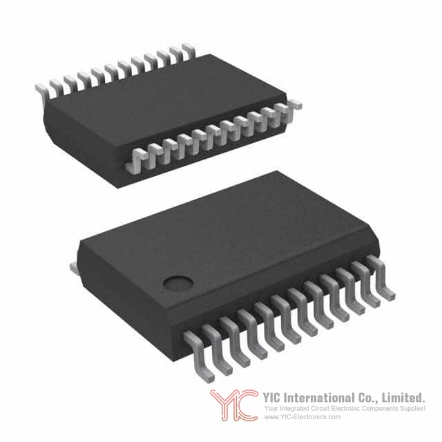
The STP16CPPS05PTR is packaged in a 24-pin TSSOP (Thin Shrink Small Outline Package) with an exposed thermal pad, providing a compact footprint suitable for space-constrained applications. The pin configuration includes dedicated signal pins for power, ground, data input/output, control signals, and LED outputs.
The power supply pins (VDD and VSS) establish the operating voltage for the device. The STP16CPPS05PTR accepts supply voltages from 3 V to 5 V, with the device automatically adjusting its internal reference circuits to maintain consistent output current across this range. The exposed thermal pad on the package bottom must be soldered directly to the PCB ground plane to achieve the thermal performance benefits documented in the datasheet.
The serial data input (SDI) pin receives data from the microcontroller or upstream shift register stage. Data is sampled on the rising edge of the clock signal (CLK), allowing synchronous operation with standard microcontroller SPI interfaces. The serial data output (SDO) pin provides the shifted data for cascading multiple STP16CPPS05PTR devices—a configuration where the SDO of one device connects to the SDI of the next, enabling control of 32, 48, or more LED channels from a single microcontroller interface.
The latch enable (LE) pin controls when the shift register contents transfer to the storage register. When LE is held low, the storage register maintains its previous state regardless of shift register activity. Transitioning LE to high level captures the current shift register contents into the storage register, updating all 16 outputs simultaneously. This level-sensitive operation (not edge-triggered) allows flexible timing control.
The output enable (OE) pin provides active-low control over the output stage. When OE is held low, the 16 output pins respond to the data stored in the latch register—either driving current (logic 1) or sinking to ground (logic 0). When OE transitions to high level, all 16 outputs are forced off, regardless of latch contents. This pin is typically driven by a PWM signal to implement brightness control through pulse-width modulation.
The 16 output pins (OUT0 through OUT15) are the current sink terminals where LEDs connect. Each output can sink up to 40 mA of constant current, with the actual current level set by an external resistor connected to the REXT pin. The outputs are designed to operate with LED forward voltages up to 20 V, allowing multiple LEDs to be connected in series on each channel.
Power Supply and Thermal Management Specifications for the STP16CPPS05PTR
The STP16CPPS05PTR operates across a wide supply voltage range from 3 V to 5 V, accommodating both 3.3 V and 5 V logic systems without external level shifters. This flexibility simplifies system design by eliminating the need for separate power domains or voltage translation circuits. The device maintains output current accuracy across this entire supply range through internal compensation circuits.
Thermal management is a critical consideration in LED driver applications, particularly when driving multiple channels at high current levels. The STP16CPPS05PTR is available in multiple package options, with the TSSOP24 exposed pad variant providing superior thermal performance. The exposed pad increases heat dissipation capability by a factor of 2.5 compared to standard TSSOP packages, achieved by providing a direct thermal path from the die to the PCB ground plane.
The thermal resistance from junction to ambient (θJA) for the TSSOP24 exposed pad package is approximately 60°C/W when the exposed pad is properly soldered to a PCB ground plane. This specification assumes a standard PCB with adequate copper area for heat spreading. The junction-to-case thermal resistance (θJC) is approximately 20°C/W, indicating efficient heat transfer from the die to the package exterior.
Power dissipation in the STP16CPPS05PTR occurs in two primary locations: the shift register and latch circuits consume minimal power during normal operation, while the output current source stages dissipate the majority of power. The power dissipation is directly proportional to the output current and the voltage drop across each output stage. For example, driving 16 channels at 20 mA each with a 5 V supply and 3 V LED forward voltage results in approximately 1.6 W of power dissipation in the output stages.
The device includes thermal shutdown protection that automatically disables the output stages if the junction temperature exceeds approximately 150°C, preventing permanent damage from thermal runaway. This protection is automatic and requires no external intervention, though proper PCB thermal design should prevent this condition from occurring during normal operation.
Output Current Control and Adjustment in the STP16CPPS05PTR
The STP16CPPS05PTR provides adjustable output current through an external resistor connected to the REXT pin. This approach offers several advantages over fixed-current designs: it allows system designers to optimize LED brightness for specific applications without requiring different IC variants, and it enables field adjustment of brightness levels through resistor selection.
The output current is set according to the relationship between the REXT resistor value and the internal reference voltage. The device maintains a constant voltage across the REXT resistor, typically around 0.5 V, creating a current proportional to the reciprocal of the resistance value. The output current can be adjusted from 3 mA to 40 mA by selecting appropriate REXT values.
The typical current accuracy of the STP16CPPS05PTR is ±5% across the operating temperature range and supply voltage range, ensuring consistent LED brightness across production batches and throughout the device's operational life. This accuracy specification assumes proper PCB layout with the REXT resistor located close to the IC and connected with short traces to minimize parasitic effects.
The output current remains constant regardless of the LED forward voltage, as long as the supply voltage exceeds the LED forward voltage plus the minimum dropout voltage of the output stage. The dropout voltage—the minimum voltage difference required between the supply and LED for proper current regulation—is approximately 1.5 V at 40 mA output current and 3.3 V supply voltage. This specification is important for applications using multiple LEDs in series, as it determines the maximum number of LEDs that can be driven from a given supply voltage.
The STP16CPPS05PTR provides independent current control for each of the 16 output channels through the shift register data. Each bit in the shift register corresponds to one output channel: a logic 1 enables the current source for that channel, while a logic 0 disables it. This binary on/off control, combined with external PWM applied to the OE pin, enables full brightness control from 0% to 100% through software control.
Serial Data Processing and Shift Register Operation in the STP16CPPS05PTR
The STP16CPPS05PTR incorporates a 16-bit serial-in, parallel-out shift register that accepts data sequentially from a microcontroller or upstream device. Data entry begins with the first bit applied to the SDI pin, which is captured on the rising edge of the clock signal. Each subsequent clock pulse shifts the data through the register, with new data entering at SDI and the oldest data exiting at SDO.
The shift register operates at clock frequencies up to 30 MHz, enabling rapid data updates. This high clock frequency is particularly valuable in cascaded configurations where multiple STP16CPPS05PTR devices are chained together. For example, controlling 48 LED channels (three cascaded devices) requires only 48 clock pulses to update all outputs, a process that completes in less than 2 microseconds at 30 MHz clock frequency.
The serial data output (SDO) pin provides the shifted data for cascading applications. The SDO output is synchronized with the clock signal and can directly drive the SDI input of a downstream STP16CPPS05PTR device. This cascading capability allows systems to scale from 16 channels to hundreds of channels using a single microcontroller interface, with each additional device requiring only one additional SDO-to-SDI connection.
The timing relationships between clock, data input, and data output are precisely defined to ensure reliable operation. The data setup time (the minimum time data must be stable before the clock edge) is typically 10 ns, while the data hold time (the minimum time data must remain stable after the clock edge) is typically 5 ns. These timing specifications are well within the capabilities of standard microcontroller SPI interfaces, which typically provide setup and hold times of 50 ns or greater.
Latch and Output Enable Control Mechanisms in the STP16CPPS05PTR
The latch enable (LE) signal controls the transfer of data from the shift register to the storage register, determining when the 16 output channels update. The LE signal is level-sensitive rather than edge-triggered, meaning the storage register captures shift register data whenever LE is held high. This level-sensitive operation provides flexibility in system design: the LE signal can be held high continuously during data entry, with the storage register automatically capturing the final data state when all 16 bits have been shifted in.
The typical sequence for updating outputs involves three steps. First, the microcontroller holds LE low to prevent the storage register from capturing incomplete data. Second, the microcontroller clocks 16 bits of data into the shift register through the SDI pin. Third, the microcontroller transitions LE to high level, capturing the shift register contents into the storage register and updating all 16 outputs simultaneously. This atomic update prevents visual artifacts that would occur if outputs updated sequentially as data was shifted in.
The output enable (OE) pin provides independent control over whether the latched data drives the output stages. When OE is held low, the 16 output pins respond to the storage register contents. When OE transitions to high level, all 16 outputs are forced off, sinking no current regardless of the stored data. This pin is typically driven by a PWM signal to implement brightness control.
The brightness control through OE pulse-width modulation works by rapidly toggling the OE signal between high and low states. For example, a 50% brightness level is achieved by holding OE low for 50% of a PWM period and high for the remaining 50%. The human eye integrates the on/off cycles, perceiving an average brightness proportional to the duty cycle. PWM frequencies above 100 Hz are typically used to avoid visible flicker, with frequencies of 1 kHz or higher providing smooth brightness transitions.
The combination of LE and OE control enables sophisticated display management. The LE signal allows rapid updates of all 16 channels simultaneously, while the OE signal provides independent brightness control. This separation of concerns simplifies firmware implementation and allows brightness adjustments without requiring new data to be shifted into the device.
Timing Characteristics and Data Transfer in the STP16CPPS05PTR
The STP16CPPS05PTR defines precise timing relationships between all control signals to ensure reliable operation across temperature and supply voltage variations. The clock frequency can range from DC (static levels) to 30 MHz, accommodating both slow, bit-banged interfaces and high-speed SPI implementations.
The setup time for serial data is the minimum duration that data must be stable before the rising clock edge. For the STP16CPPS05PTR, this specification is typically 10 ns, meaning data should be valid at least 10 ns before the clock edge. The hold time is the minimum duration data must remain stable after the clock edge, typically 5 ns. These specifications ensure that data is reliably captured by the shift register flip-flops.
The propagation delay from clock input to serial data output (the time required for data to appear at SDO after a clock pulse) is typically 15 ns. This specification is important in cascaded configurations, as it determines the maximum clock frequency that can be used while maintaining reliable data transfer between devices. When cascading multiple STP16CPPS05PTR devices, the propagation delay of one device must be less than the setup time of the next device, a condition easily satisfied at clock frequencies up to 30 MHz.
The output enable response time—the delay from when OE transitions to when the output stages respond—is typically 50 ns for turn-on and 30 ns for turn-off. These response times are fast enough for PWM brightness control at frequencies up to several kilohertz without visible artifacts.
The latch enable timing is level-sensitive, meaning the storage register captures data whenever LE is high. The setup and hold times for the latch operation are typically 10 ns and 5 ns respectively, measured relative to the clock signal. This timing ensures that the storage register captures stable data from the shift register.
Auto Power-Saving Functionality of the STP16CPPS05PTR
The STP16CPPS05PTR incorporates an auto power-saving feature that automatically reduces power consumption when no active data is present in the storage register. This feature is particularly valuable in battery-powered applications or systems where LED displays are inactive for extended periods.
The auto power-saving mechanism monitors the contents of the storage register. When all 16 bits are zero (all outputs off), the device automatically enters shutdown mode, reducing the quiescent current from approximately 4.2 mA in normal operation to approximately 190 microamperes in shutdown mode. This represents a 22-fold reduction in power consumption, a significant benefit for portable devices or always-on displays that spend extended periods in the off state.
The transition from shutdown mode to normal operation is automatic and requires no external intervention. When the first active data bit (a logic 1) is latched into the storage register, the device automatically powers up the output stages and returns to normal operation. The turn-on process includes a brief startup transient where the first output to activate shows a slightly extended rise time, typically 100 ns longer than subsequent outputs. This transient is a minor effect that does not impact display functionality.
The auto power-saving feature operates continuously and transparently to the system firmware. No configuration or control signals are required to enable or disable the feature—it is always active. This automatic operation simplifies system design by eliminating the need for firmware to manage power states.
The power consumption reduction provided by auto power-saving is particularly valuable in applications such as LED signage, where displays may be off for 16 hours per day. A system with 10 STP16CPPS05PTR devices consuming 190 microamperes each in shutdown mode draws only 1.9 mA during off periods, compared to 42 mA in normal operation. Over a 16-hour off period, this represents a power savings of approximately 0.65 Watt-hours per day, or 237 Watt-hours per year—a meaningful reduction in energy consumption and operating cost.
Package Options and Thermal Performance of the STP16CPPS05PTR
The STP16CPPS05PTR is available in multiple package options to accommodate different application requirements and thermal constraints. The primary package variant is the TSSOP24 (Thin Shrink Small Outline Package) with an exposed thermal pad, which provides the optimal balance of thermal performance and PCB area efficiency.
The TSSOP24 exposed pad package measures 6.4 mm × 4.4 mm, providing a compact footprint suitable for space-constrained applications. The exposed pad on the package bottom provides a direct thermal path from the die to the PCB ground plane, increasing heat dissipation capability by a factor of 2.5 compared to standard TSSOP packages without exposed pads. This thermal enhancement is achieved through proper PCB design: the exposed pad must be soldered directly to a copper land on the PCB ground plane, with adequate copper area (typically 20 mm² or larger) to spread heat effectively.
The mechanical specifications for the TSSOP24 exposed pad package define precise dimensions for PCB land patterns, solder mask openings, and copper area requirements. The exposed pad land should be slightly smaller than the package pad to ensure proper solder wetting and prevent solder bridges to adjacent pins. The PCB ground plane should extend at least 5 mm in all directions from the package to provide adequate heat spreading.
Alternative package options include the standard TSSOP24 (without exposed pad), the SO-24 (Small Outline), and the QSOP-24 (Quarter-size Small Outline). These alternatives provide lower thermal performance but may be preferred in applications where thermal constraints are less stringent or where PCB space is extremely limited.
The thermal resistance specifications for the TSSOP24 exposed pad package assume proper PCB design with adequate copper area and thermal vias connecting the exposed pad to internal ground planes. The junction-to-ambient thermal resistance (θJA) is approximately 60°C/W under these conditions. For applications requiring lower thermal resistance, multiple thermal vias (typically 0.3 mm diameter) should be placed under the exposed pad, with via spacing of 0.5 mm to 1 mm. Each via provides approximately 0.5°C/W of additional thermal conductance, allowing thermal resistance to be reduced to 40°C/W or lower with proper via design.
The power dissipation characteristics of the STP16CPPS05PTR vary with output current and supply voltage. At maximum output current (40 mA on all 16 channels) with a 5 V supply and 3 V LED forward voltage, the device dissipates approximately 3.2 W. With proper thermal design using the TSSOP24 exposed pad package and thermal vias, the junction temperature rise above ambient would be approximately 192°C, requiring an ambient temperature below -42°C to maintain safe operation—clearly impractical. In such high-power applications, the system design must either reduce the output current, use a lower supply voltage, or employ external heat sinking.
More typical applications operate at lower output currents. For example, driving 16 channels at 10 mA each with a 5 V supply and 3 V LED forward voltage results in approximately 0.8 W of power dissipation, producing a junction temperature rise of approximately 48°C above ambient. This is easily managed with the TSSOP24 exposed pad package in typical room-temperature environments.
Conclusion
The STP16CPPS05PTR represents a mature, well-optimized solution for LED display applications requiring 16 channels of constant current control. The device combines a high-speed serial interface with independent output control, enabling flexible brightness management and cascading capability for larger displays. The wide supply voltage range (3 V to 5 V) and low-voltage operation make the STP16CPPS05PTR suitable for both legacy systems and modern microcontroller environments. The auto power-saving feature provides significant energy efficiency benefits in applications where displays are inactive for extended periods. The availability of multiple package options, particularly the TSSOP24 exposed pad variant with enhanced thermal performance, allows designers to optimize for their specific thermal and space constraints. The combination of these features—constant current regulation, adjustable output current, high-speed serial interface, and automatic power management—makes the STP16CPPS05PTR a practical choice for LED panel displays, indicator arrays, and other applications requiring precise, efficient LED control.
Frequently Asked Questions (FAQ)
- Q1. What is the maximum number of LEDs that can be driven from a single STP16CPPS05PTR output channel?
-
- A1. The maximum number of LEDs depends on the supply voltage and the LED forward voltage. Each STP16CPPS05PTR output can maintain constant current with LED forward voltages up to 20 V. For example, with a 5 V supply and 3.3 V LED forward voltage, approximately one LED can be driven per channel. With a 24 V supply and 3.3 V LED forward voltage, approximately seven LEDs in series can be driven per channel. The limiting factor is the dropout voltage of the output stage, which is approximately 1.5 V at 40 mA. The formula is: Maximum LEDs = (Supply Voltage - Dropout Voltage) / LED Forward Voltage.
- Q2. Can multiple STP16CPPS05PTR devices be cascaded to control more than 16 LED channels?
-
- A2. Yes, multiple STP16CPPS05PTR devices can be cascaded by connecting the serial data output (SDO) of one device to the serial data input (SDI) of the next device. All devices share the same clock and latch enable signals. For example, three cascaded devices provide 48 LED channels. The cascading is limited only by the microcontroller's ability to generate the required clock frequency and the propagation delays through the shift registers. At 30 MHz clock frequency, updating 48 channels requires less than 2 microseconds.
- Q3. How is brightness control implemented in the STP16CPPS05PTR?
-
- A3. Brightness control is implemented through pulse-width modulation (PWM) of the output enable (OE) pin. By rapidly toggling the OE signal between high (outputs off) and low (outputs on), the average current delivered to the LEDs is proportional to the duty cycle. For example, a 50% duty cycle produces 50% brightness. PWM frequencies above 100 Hz are typically used to avoid visible flicker. The shift register data provides binary on/off control for each channel, while the OE signal provides analog brightness control for all channels simultaneously.
- Q4. What is the purpose of the external REXT resistor, and how is it selected?
-
- A4. The external REXT resistor sets the output current level for all 16 channels. The device maintains a constant voltage across the REXT resistor, creating a current proportional to the reciprocal of the resistance value. The output current can range from 3 mA to 40 mA by selecting appropriate REXT values. For example, to achieve 20 mA output current, an REXT value of approximately 25 kΩ is required. The exact relationship between REXT and output current is provided in the datasheet's typical characteristics section. The REXT resistor should be located close to the IC with short traces to minimize parasitic effects.
- Q5. What are the advantages of the auto power-saving feature?
-
- A5. The auto power-saving feature automatically reduces power consumption from approximately 4.2 mA to 190 microamperes when all outputs are off. This 22-fold reduction in quiescent current is particularly valuable in battery-powered applications or systems where displays are inactive for extended periods. The feature operates automatically without requiring firmware intervention. For example, a system with 10 STP16CPPS05PTR devices saves approximately 237 Watt-hours per year if the display is off for 16 hours per day.
- Q6. How should the exposed thermal pad be connected for optimal thermal performance?
-
- A6. The exposed thermal pad on the TSSOP24 exposed pad package must be soldered directly to a copper land on the PCB ground plane. The copper land should be at least 20 mm² in area, with the PCB ground plane extending at least 5 mm in all directions from the package. For applications with high power dissipation, multiple thermal vias (typically 0.3 mm diameter) should be placed under the exposed pad, with via spacing of 0.5 mm to 1 mm. Each via provides approximately 0.5°C/W of additional thermal conductance. Proper thermal design can reduce the junction-to-ambient thermal resistance from 60°C/W to 40°C/W or lower.
- Q7. What is the typical current accuracy of the STP16CPPS05PTR across temperature and supply voltage variations?
-
- A7. The typical current accuracy is ±5% across the operating temperature range (0°C to 70°C) and supply voltage range (3 V to 5 V). This accuracy specification ensures consistent LED brightness across production batches and throughout the device's operational life. The accuracy assumes proper PCB layout with the REXT resistor located close to the IC and connected with short traces to minimize parasitic effects.
- Q8. What clock frequency should be used for reliable cascading of multiple STP16CPPS05PTR devices?
-
- A8. The STP16CPPS05PTR supports clock frequencies up to 30 MHz. For cascading applications, the propagation delay from one device's SDO to the next device's SDI must be less than the setup time of the receiving device. At 30 MHz clock frequency, the propagation delay of approximately 15 ns is well within the setup time requirement of 10 ns, allowing reliable cascading. In practice, clock frequencies of 10 MHz to 20 MHz are commonly used for cascading to provide timing margin and reduce EMI.
- Q9. How does the STP16CPPS05PTR maintain constant output current despite variations in LED forward voltage?
-
- A9. The STP16CPPS05PTR uses regulated current source circuits in the output stage. These circuits continuously monitor the output current and adjust the internal resistance to maintain the target current level set by the REXT resistor. As the LED forward voltage changes due to temperature variations or LED aging, the current source automatically adjusts to maintain constant current. This regulation works as long as the supply voltage exceeds the LED forward voltage plus the dropout voltage (approximately 1.5 V at 40 mA).
- Q10. What is the minimum supply voltage required for the STP16CPPS05PTR to operate reliably?
-
- A10. The minimum supply voltage is 3 V. However, the practical minimum supply voltage depends on the LED forward voltage and the desired output current. The supply voltage must exceed the LED forward voltage plus the dropout voltage of the output stage. For example, with a 3 V LED forward voltage and 40 mA output current (dropout voltage approximately 1.5 V), the minimum supply voltage would be approximately 4.5 V. For lower output currents, the dropout voltage is lower, allowing operation with lower supply voltages. The datasheet provides detailed dropout voltage specifications for various output current levels.
- Q11. Can the STP16CPPS05PTR be used with 3.3 V microcontroller logic levels?
-
- A11. Yes, the STP16CPPS05PTR is specifically designed for 3.3 V microcontroller compatibility. The device can operate with a 3.3 V supply and accepts 3.3 V logic levels on all input pins (SDI, CLK, LE, OE). The input thresholds are designed to reliably detect 3.3 V logic signals. This eliminates the need for level shifters when interfacing with 3.3 V microcontrollers, simplifying system design and reducing component count.
- Q12. What is the typical turn-on and turn-off response time of the output stage?
-
- A12. The output enable response time is typically 50 ns for turn-on (when OE transitions from high to low) and 30 ns for turn-off (when OE transitions from low to high). These response times are fast enough for PWM brightness control at frequencies up to several kilohertz without visible artifacts. The turn-on response time is slightly longer than turn-off due to the current source charging the output capacitance. These timing specifications are important for applications requiring precise brightness control or synchronized multi-device operation.