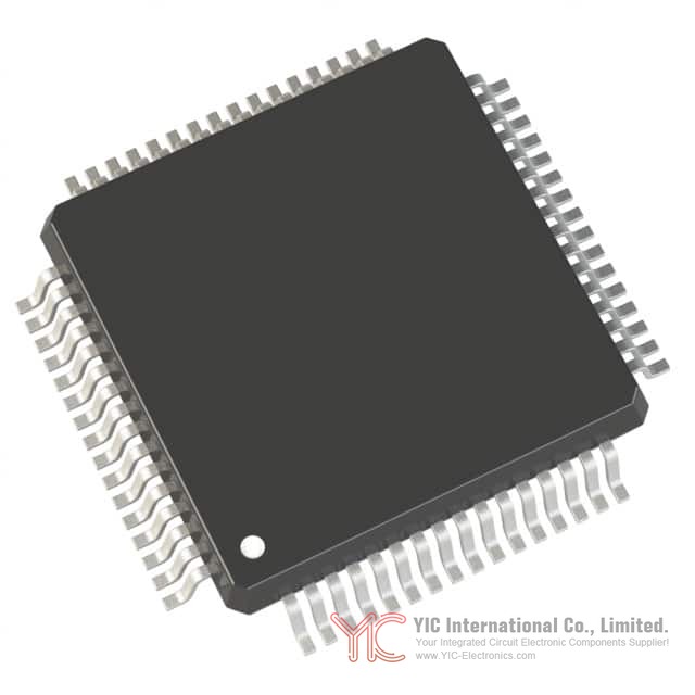
Product Overview of the SPC560B40x/50x and SPC560C40x/50x Series
The SPC560B40x/50x and SPC560C40x/50x series represents a family of 32-bit microcontrollers specifically engineered for automotive body electronics applications. Built on the Power Architecture embedded category, these devices combine high-performance processing with integrated automotive-grade peripherals to address the evolving demands of vehicle control systems.
The SPC560B40x/50x and SPC560C40x/50x family delivers a balanced approach to automotive controller design, offering sufficient processing power for complex body electronics tasks while maintaining cost efficiency. The architecture supports variable-length encoding (VLE) through its APU implementation, which improves code density and allows developers to optimize memory utilization in flash-constrained applications.
Core Architecture and Processing Capabilities of the SPC560B40x/50x and SPC560C40x/50x
At the heart of the SPC560B40x/50x and SPC560C40x/50x series lies the e200z0h CPU, a 32-bit processor operating at frequencies up to 64 MHz. This core delivers up to 60 DMIPs (Dhrystone Million Instructions Per Second) of processing performance, providing sufficient computational capacity for real-time control tasks typical in automotive body electronics.
The processor implements the Power Architecture instruction set with VLE support, enabling more compact code representation compared to traditional fixed-length instruction architectures. This becomes particularly valuable in applications where flash memory is limited, as developers can fit more functionality within the same memory footprint. The architecture maintains compatibility with existing Power Architecture development tools and software infrastructure, reducing the learning curve for teams already familiar with this processor family.
Memory Organization in the SPC560B40x/50x and SPC560C40x/50x Series
The SPC560B40x/50x and SPC560C40x/50x devices incorporate a hierarchical memory structure designed to balance performance with cost. Code flash memory ranges up to 512 KB with error-correcting code (ECC) protection, ensuring data integrity across the device lifetime. The ECC circuitry automatically corrects single-bit faults, improving reliability in automotive environments where electromagnetic interference and temperature variations can introduce transient errors.
Data flash memory of 64 KB provides non-volatile storage for calibration parameters, configuration data, and other application-specific information that must persist across power cycles. This separation of code and data flash allows independent management of program updates and parameter storage, simplifying firmware maintenance procedures.
The SPC560B40x/50x and SPC560C40x/50x series includes up to 48 KB of SRAM with ECC protection. This volatile memory serves as the primary workspace for runtime data, stack operations, and temporary variables. The ECC protection extends to SRAM as well, maintaining data integrity throughout the device operation. An 8-entry memory protection unit (MPU) provides hardware-enforced memory access control, enabling separation of critical code regions and preventing accidental or malicious memory corruption.
Clock Generation and Oscillator Options for the SPC560B40x/50x and SPC560C40x/50x
The SPC560B40x/50x and SPC560C40x/50x series provides multiple clock sources to accommodate various application requirements and power management strategies. The fast external crystal oscillator (FXOSC) accepts input frequencies from 4 to 16 MHz, allowing integration with standard crystal components available in the market. This oscillator drives the frequency-modulated phase-locked loop (FMPLL), which generates the high-speed system clock through programmable multiplication factors.
For applications requiring real-time clock functionality, the SPC560B40x/50x and SPC560C40x/50x include a 32 kHz slow external crystal oscillator (SXOSC). This low-frequency clock source consumes minimal power while maintaining accurate timekeeping, making it suitable for applications that need to track time during low-power standby modes.
The SPC560B40x/50x and SPC560C40x/50x incorporate internal oscillators as well. A 16 MHz fast internal RC oscillator (FIRC) serves as the default clock source at power-up, enabling immediate code execution without waiting for external crystal stabilization. A 128 kHz slow internal RC oscillator (SIRC) provides a low-power clock option for reduced-frequency operation during standby modes. The clock monitor unit (CMU) continuously validates the integrity of the selected clock source, triggering a reset if clock failure is detected.
Communication Interfaces in the SPC560B40x/50x and SPC560C40x/50x
The SPC560B40x/50x and SPC560C40x/50x series integrates multiple communication interfaces to support diverse connectivity requirements in automotive systems. Up to six FlexCAN interfaces implement the CAN 2.0B protocol with 64-message objects per interface, enabling robust vehicle network communication. The CAN implementation supports both standard and extended identifier formats, accommodating various network topologies and message prioritization schemes.
For serial communication, the SPC560B40x/50x and SPC560C40x/50x provide up to four LINFlex/UART interfaces. These interfaces support both LIN (Local Interconnect Network) protocol for low-speed body electronics networks and standard UART operation for general-purpose serial communication. The LINFlex implementation includes automatic baud rate detection, simplifying integration with LIN network nodes.
The SPC560B40x/50x and SPC560C40x/50x include three DSPI (Deserial Serial Peripheral Interface) modules capable of operating as SPI master or slave. These interfaces support both classic SPI timing and modified transfer formats, with configurable clock phases and polarities. The DSPI modules can operate at frequencies up to the system clock rate, enabling high-speed data transfers with external peripherals such as sensors, memory devices, and display controllers.
Analog Signal Processing: ADC Implementation in the SPC560B40x/50x and SPC560C40x/50x
The SPC560B40x/50x and SPC560C40x/50x series incorporates a 10-bit successive approximation register (SAR) analog-to-digital converter with up to 36 dedicated input channels. The ADC architecture supports both precise channels with low input leakage and extended channels accessible through external multiplexing, allowing expansion to 64 total channels when needed.
The ADC includes a cross-triggering unit (CTU) that enables synchronized analog measurements with timer events or other system triggers. This capability proves valuable in applications requiring synchronized sampling of multiple analog signals, such as motor control or power management systems. The ADC diagnostic module provides time-triggered measurements for system health monitoring, allowing continuous verification of sensor functionality.
Input impedance considerations become important when designing analog signal conditioning circuits. The ADC sampling capacitance creates a charge-sharing effect with external filter capacitors, requiring careful circuit design to maintain measurement accuracy. The device documentation provides detailed analysis of these effects, including equations for calculating appropriate filter component values based on source impedance and desired accuracy.
Timer and Counter Functions in the SPC560B40x/50x and SPC560C40x/50x
The SPC560B40x/50x and SPC560C40x/50x series provides comprehensive timing capabilities through multiple timer modules. Six 32-bit periodic interrupt timers generate regular interrupts at programmable intervals, supporting real-time scheduling and periodic task execution. A four-channel 32-bit system timer module (STM) offers additional timing flexibility for applications requiring multiple independent time bases.
The SPC560B40x/50x and SPC560C40x/50x include a software watchdog timer that monitors code execution and triggers a reset if the watchdog is not serviced within a specified time window. This mechanism protects against runaway code execution caused by electromagnetic interference or software errors. A real-time clock timer maintains accurate time tracking across power cycles when supplied with the 32 kHz oscillator.
The SPC560B40x/50x and SPC560C40x/50x feature 16-bit counter time-triggered I/Os with up to 56 channels supporting PWM (pulse-width modulation), modulus counter, input capture, and output compare functions. These channels enable precise control of motor drives, lighting systems, and other actuators common in automotive body electronics. The PWM generation includes advanced features such as synchronized ADC triggering and diagnostic output capabilities.
Power Management and Low-Power Modes in the SPC560B40x/50x and SPC560C40x/50x
The SPC560B40x/50x and SPC560C40x/50x series implements a sophisticated power management architecture supporting multiple operating modes. The RUN mode provides full performance at up to 64 MHz for active processing tasks. STOP mode reduces power consumption by disabling the main clock while maintaining RAM and register contents, enabling rapid wake-up when needed.
The SPC560B40x/50x and SPC560C40x/50x support ultra-low power STANDBY mode, which maintains the real-time clock, selected SRAM regions, and CAN monitoring capability while minimizing overall power consumption. This mode proves valuable for applications requiring continuous network presence with minimal power draw, such as vehicle security systems or remote diagnostics modules.
An internal voltage regulator generates the 1.2 V core supply from the external 3.3 V or 5.0 V input, with separate ballast and core supply domains to minimize noise coupling. The regulator requires external decoupling capacitors on three dedicated VDD_LV/VSS_LV supply pairs to ensure stable operation. Low voltage detectors monitor both the main supply and internal core supply, triggering controlled resets if voltage drops below safe operating levels.
Input/Output Architecture and Pin Configuration of the SPC560B40x/50x and SPC560C40x/50x
The SPC560B40x/50x and SPC560C40x/50x series provides flexible I/O capabilities through multiple package options. The LQFP64 package offers 45 GPIO pins, while the LQFP100 package provides 75 GPIO pins and the LQFP144 package delivers 123 GPIO pins. This range allows designers to select the appropriate package size based on application requirements.
The SPC560B40x/50x and SPC560C40x/50x implement four types of I/O pads optimized for different performance requirements. Slow pads provide a good compromise between transition speed and electromagnetic emission, suitable for general-purpose I/O. Medium pads offer faster transitions for serial communication interfaces while maintaining controlled current to reduce EMI. Fast pads provide maximum speed for debugging interfaces. Input-only pads associated with ADC channels and oscillator inputs minimize leakage current.
All I/O pads support configurable pull-up and pull-down resistors, allowing external pull resistors to be eliminated in many applications. The pads can be configured for different output drive strengths through the slew rate control (SRC) bits, enabling optimization of signal integrity and EMI performance for specific applications.
Package Options and Mechanical Specifications for the SPC560B40x/50x and SPC560C40x/50x
The SPC560B40x/50x and SPC560C40x/50x series is available in four package options to accommodate different application requirements. The LQFP64 package measures 10 x 10 x 1.4 mm and provides 64 pins on 0.5 mm pitch, suitable for space-constrained applications. The LQFP100 package measures 14 x 14 x 1.4 mm with 100 pins, offering expanded I/O capability while maintaining a compact footprint.
The LQFP144 package measures 20 x 20 x 1.4 mm with 144 pins, providing maximum I/O count for applications requiring extensive peripheral connectivity. An LBGA208 package is available as a development platform for advanced debugging through Nexus 2+ interface, though this package is not intended for production applications.
All packages comply with ECOPACK environmental standards, meeting RoHS and other environmental regulations. The mechanical specifications include detailed dimensional data, pin assignments, and thermal characteristics necessary for PCB layout and thermal management calculations.
Electrical Characteristics and Operating Conditions for the SPC560B40x/50x and SPC560C40x/50x
The SPC560B40x/50x and SPC560C40x/50x series operates from either 3.3 V or 5.0 V external supplies, with the internal regulator generating the 1.2 V core supply. The device maintains full functionality across the temperature range from -40°C to 125°C, covering automotive ambient and junction temperature extremes.
I/O pad electrical characteristics vary based on pad type and configuration. Input thresholds are specified for both 3.3 V and 5.0 V operation, with hysteresis to improve noise immunity. Output drive capability depends on the selected pad configuration, with slow pads providing lower current but reduced EMI, while fast pads deliver higher current for demanding loads.
The SPC560B40x/50x and SPC560C40x/50x implement ESD protection on all I/O pins, with absolute maximum ratings specified for electrostatic discharge events. Latch-up testing confirms the device's immunity to parasitic thyristor activation under worst-case current injection conditions. These electrical protections ensure reliable operation in harsh automotive environments.
Power consumption varies significantly based on operating mode and peripheral utilization. RUN mode consumption depends on clock frequency and active peripherals, ranging from approximately 20 mA at 64 MHz with typical peripherals active to lower values when operating at reduced frequencies or with peripherals disabled. STOP mode reduces consumption to the low milliamp range, while STANDBY mode achieves microamp-level consumption with RTC and CAN monitoring active.
Debugging and Development Support in the SPC560B40x/50x and SPC560C40x/50x
The SPC560B40x/50x and SPC560C40x/50x series includes Nexus 1 debugging capability on all devices, providing real-time code execution visibility and breakpoint support. The LBGA208 development package adds Nexus 2+ capability with eight additional debug pins, enabling advanced trace and profiling features for complex application development.
JTAG boundary scan support enables in-circuit testing and verification of board-level connectivity. The JTAG interface operates at frequencies up to the system clock rate, supporting rapid device programming and verification during manufacturing. The TDO pad includes special handling for low-power debug handshaking in STANDBY mode, with recommendations for external pull-up resistors to prevent floating pin issues.
Conclusion
The SPC560B40x/50x and SPC560C40x/50x series delivers a comprehensive solution for automotive body electronics applications, combining a capable 32-bit processor with integrated communication interfaces, analog signal processing, and power management features. The flexible package options and configurable I/O capabilities enable designers to optimize cost and performance for specific application requirements. The robust electrical specifications and automotive-grade reliability features ensure dependable operation across the full range of vehicle operating conditions.
Frequently Asked Questions (FAQ)
- Q1. What is the maximum operating frequency of the SPC560B40x/50x and SPC560C40x/50x, and how does it affect power consumption?
-
- A1. The SPC560B40x/50x and SPC560C40x/50x operate at frequencies up to 64 MHz, delivering up to 60 DMIPs of processing performance. Power consumption scales approximately linearly with clock frequency in RUN mode. At 64 MHz with typical peripherals active, the device consumes approximately 20 mA. Reducing the clock frequency through the FMPLL multiplier or using the internal RC oscillators can significantly reduce power consumption for applications that do not require maximum performance.
- Q2. How many CAN interfaces does the SPC560B40x/50x and SPC560C40x/50x provide, and what protocols do they support?
-
- A2. The SPC560B40x/50x and SPC560C40x/50x provide up to six FlexCAN interfaces, each supporting the CAN 2.0B protocol with 64-message objects. The CAN implementation supports both standard 11-bit and extended 29-bit identifier formats, enabling integration with various vehicle network architectures. Each interface operates independently, allowing simultaneous communication on multiple CAN networks.
- Q3. What memory protection features does the SPC560B40x/50x and SPC560C40x/50x include?
-
- A3. The SPC560B40x/50x and SPC560C40x/50x incorporate an 8-entry memory protection unit (MPU) that enforces hardware-based access control. This allows separation of critical code regions and prevents accidental or malicious memory corruption. Additionally, both code flash and SRAM include error-correcting code (ECC) protection that automatically corrects single-bit errors, improving reliability in electromagnetically noisy automotive environments.
- Q4. Can the SPC560B40x/50x and SPC560C40x/50x operate from a 5.0 V supply, and are there any special considerations?
-
- A4. Yes, the SPC560B40x/50x and SPC560C40x/50x support operation from either 3.3 V or 5.0 V external supplies. When operating at 5.0 V, the internal regulator generates the 1.2 V core supply. The PAD3V5V configuration bit in the NVUSRO register controls I/O pad electrical characteristics for the selected supply voltage. Full device operation is guaranteed when voltage drops from 5.0 V to 3.0 V, though certain analog characteristics may not be guaranteed below 4.5 V.
- Q5. What is the ADC resolution and how many input channels are available on the SPC560B40x/50x and SPC560C40x/50x?
-
- A5. The SPC560B40x/50x and SPC560C40x/50x incorporate a 10-bit successive approximation register (SAR) ADC with up to 36 dedicated input channels. The ADC can be extended to 64 total channels through external multiplexing. The cross-triggering unit (CTU) enables synchronized analog measurements with timer events, supporting applications requiring coordinated sampling of multiple signals.
- Q6. How does the SPC560B40x/50x and SPC560C40x/50x handle low-power operation, and what is the standby mode consumption?
-
- A6. The SPC560B40x/50x and SPC560C40x/50x support multiple power modes including RUN, STOP, and STANDBY. STANDBY mode maintains the real-time clock, selected SRAM regions, and CAN monitoring while minimizing power consumption to the microamp range. This mode enables applications requiring continuous network presence with minimal power draw, such as vehicle security systems. The device can wake from STANDBY through external interrupts or CAN message reception.
- Q7. What communication interfaces are available on the SPC560B40x/50x and SPC560C40x/50x for serial data transfer?
-
- A7. The SPC560B40x/50x and SPC560C40x/50x provide up to four LINFlex/UART interfaces for serial communication and up to three DSPI modules for SPI operation. The LINFlex interfaces support both LIN protocol for low-speed body electronics networks and standard UART operation. The DSPI modules support both classic SPI timing and modified transfer formats, with configurable clock phases and polarities for compatibility with various peripheral devices.
- Q8. What package options are available for the SPC560B40x/50x and SPC560C40x/50x, and how do they differ in pin count?
-
- A8. The SPC560B40x/50x and SPC560C40x/50x are available in four packages: LQFP64 with 64 pins and 45 GPIO, LQFP100 with 100 pins and 75 GPIO, LQFP144 with 144 pins and 123 GPIO, and LBGA208 with 208 pins for development purposes. The LQFP64 package measures 10 x 10 mm, LQFP100 measures 14 x 14 mm, and LQFP144 measures 20 x 20 mm, allowing selection based on application I/O requirements and PCB space constraints.
- Q9. How does the internal voltage regulator in the SPC560B40x/50x and SPC560C40x/50x function, and what external components are required?
-
- A9. The SPC560B40x/50x and SPC560C40x/50x incorporate an internal voltage regulator that generates the 1.2 V core supply from the external 3.3 V or 5.0 V input. The regulator requires external decoupling capacitors on three dedicated VDD_LV/VSS_LV supply pairs to ensure stable operation. Recommended capacitance values are 330 nF for each pair, placed as close as possible to the device pins to minimize board inductance. Additional capacitance on the VDD_BV pin helps manage in-rush current during power-up and standby exit.
- Q10. What debugging capabilities does the SPC560B40x/50x and SPC560C40x/50x provide for development and production testing?
-
- A10. The SPC560B40x/50x and SPC560C40x/50x include Nexus 1 debugging capability on all devices, providing real-time code execution visibility and breakpoint support. The LBGA208 development package adds Nexus 2+ capability with eight additional debug pins for advanced trace and profiling. JTAG boundary scan support enables in-circuit testing and verification of board-level connectivity, with the JTAG interface operating at frequencies up to the system clock rate for rapid device programming during manufacturing.
- Q11. What are the temperature operating range and thermal characteristics of the SPC560B40x/50x and SPC560C40x/50x?
-
- A11. The SPC560B40x/50x and SPC560C40x/50x operate across the temperature range from -40°C to 125°C, covering automotive ambient and junction temperature extremes. The junction-to-ambient thermal resistance varies by package type, with LQFP packages providing thermal resistance values suitable for passive cooling in typical automotive applications. Thermal management calculations should account for both internal power dissipation and I/O power dissipation when determining required cooling solutions.
- Q12. How does the SPC560B40x/50x and SPC560C40x/50x handle clock monitoring and what happens if a clock failure is detected?
-
- A12. The SPC560B40x/50x and SPC560C40x/50x include a clock monitor unit (CMU) that continuously validates the integrity of the selected clock source. If clock failure is detected, the CMU triggers a reset, preventing execution of corrupted code. This mechanism protects against electromagnetic interference that could disrupt oscillator operation. The device supports multiple clock sources including external crystals and internal RC oscillators, allowing fallback to alternative clocks if the primary source fails.