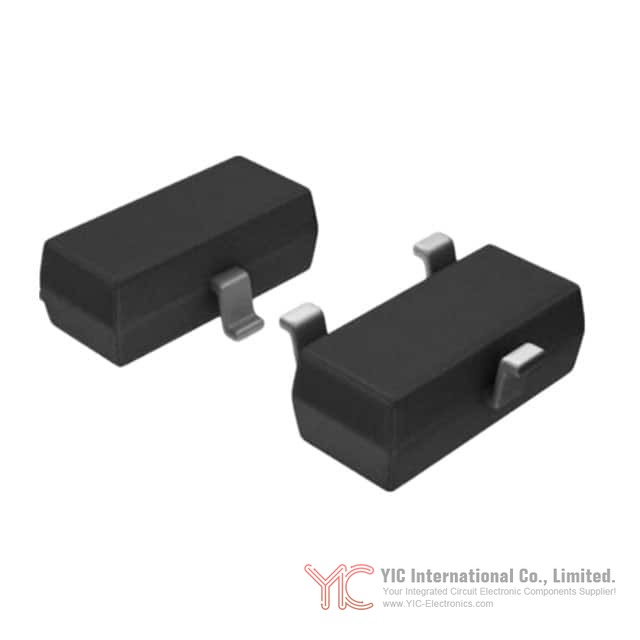
Product overview – SM712 TVS diode
The SM712 TVS diode is a surface-mount transient voltage suppressor designed to clamp surge and transient voltages on sensitive signal lines. It provides protection by diverting surge current away from protected circuitry when line voltage exceeds its breakdown region, and it returns to a high-impedance state once the transient subsides.
With a minimum breakdown voltage of 7 V and clamp voltages of 18 V and 26 V, the SM712 TVS diode is suited to protect differential data interfaces and low-voltage lines that must withstand surge events while maintaining signal integrity. The device is offered in a compact SOT‑23 package and is specified for a peak pulse current of 12 A, enabling robust protection in space-constrained designs.
Structural and functional characteristics of the SM712 TVS diode
The SM712 TVS diode is built as a transient suppression element optimized for line protection. Its main functional role is to remain electrically transparent under normal operating conditions and switch to a low-impedance path during transients.
When line voltage remains below the minimum breakdown voltage of 7 V, the SM712 TVS diode contributes negligible leakage current, allowing signals to pass with minimal loading. When a surge raises the line voltage above its breakdown region, the device conducts, clamping the voltage to specified levels (18 V or 26 V depending on polarity or line condition) and routing surge current to ground or a reference potential. This behavior protects downstream ICs whose absolute maximum ratings are typically lower than the SM712 clamp levels.
Internally, the SM712 TVS diode is optimized for fast response to transients. In surge scenarios, the transition from high impedance to conduction occurs on the order of nanoseconds. The combination of specified breakdown and clamp voltages with a 12 A peak pulse current capability allows the SM712 to handle typical surge conditions encountered on communication and low-voltage control lines, such as those conforming to industrial and communication interface standards.
Electrical performance parameters of the SM712 TVS diode
The SM712 TVS diode’s suitability for a specific design is determined primarily by its electrical parameters. Key ratings include:
• Breakdown voltage (VBR): The SM712 TVS diode has a minimum breakdown voltage of 7 V, with a typical breakdown region around 7.5 V. This defines the threshold above which the device begins to conduct more heavily. For data or control lines nominally operating below this level (such as common differential bus voltages), this ensures normal operation remains unaffected while providing room for minor line fluctuations.
• Clamp voltages: The SM712 TVS diode specifies clamp voltages of 18 V and 26 V under surge conditions. During a transient, once breakdown is reached, the device limits the line voltage to these clamp levels. Protection-sensitive ICs typically have absolute maximum ratings below these clamps, so the SM712 is used on interfaces where those clamp voltages remain within the survivable transient range of the protected devices.
• Peak pulse current (Ipp): Rated at 12 A, the SM712 TVS diode can conduct substantial surge currents for short durations. This rating reflects the maximum surge current the device can handle under specified test waveforms without damage. In practical design, this enables the SM712 to address surges such as those generated by electrostatic discharge (ESD), electrical fast transients (EFT), or induced surge events on long cables.
• Surface-mount construction: The SM712 TVS diode is implemented in a way that supports low-inductance current paths when properly laid out on the PCB. Low parasitic inductance improves clamping performance because voltage overshoot during fast transients is reduced.
Together, these parameters guide how the SM712 TVS diode behaves in surge conditions: it begins to conduct at approximately 7–7.5 V and limits the subsequent transient to clamp levels of 18 V and 26 V while safely carrying surge currents up to 12 A.
Package, mounting, and mechanical features of the SM712 TVS diode
The SM712 TVS diode is supplied in an industry-standard SOT‑23 package, aligning with a widespread footprint familiar to PCB designers. This package style enables:
• Compact layout: The SOT‑23 form factor allows placement adjacent to connector pins or IC input pins, which shortens trace lengths between protected nodes and the protection device. Reduced trace length helps minimize parasitic inductance and voltage overshoot during surge events.
• Surface-mount assembly: The SM712 TVS diode is compatible with standard reflow processes used for SMD assembly. This supports automated high-volume production and straightforward integration into existing SMT lines.
• Pin configuration: In SOT‑23, the SM712 TVS diode pins are arranged to permit symmetrical routing for differential pairs or single-ended lines, depending on the specific application. Designers can position the device at the interface between external connectors and internal circuitry to create a defined protection boundary.
From a mechanical standpoint, the SOT‑23 package of the SM712 TVS diode also influences thermal behavior under surge. While transients are short in duration, the package must safely dissipate the associated energy. The rated 12 A peak pulse current reflects the combination of the die structure and SOT‑23 package capability under the test conditions used by the manufacturer.
Typical application scenarios of the SM712 TVS diode
The SM712 TVS diode is suited to protecting signal and communication lines that must endure surge events without degrading normal signal performance. One representative scenario involves differential data interfaces that operate around low voltages, such as those used in common industrial and building automation systems.
In such systems, long cable runs expose communication lines to ESD, induced lightning surges, and switching transients. The SM712 TVS diode can be placed close to the external connector, with each line routed through the device. When a surge appears, the SM712 clamps the voltage to 18 V or 26 V, shunting current away from the transceiver inputs. After the transient, the device reverts to its high-impedance state, allowing normal communication to resume.
Another scenario is the protection of low-voltage control or sensor lines in distributed systems. For example, a sensor node in an industrial environment connected via a twisted-pair cable to a central controller can experience surge events caused by nearby inductive load switching. With the SM712 TVS diode installed at the interface, these transient voltages are limited before reaching vulnerable ADC inputs or microcontroller pins.
In practice, the SM712 TVS diode is typically positioned:
• At the boundary between external field wiring and internal electronics.
• On each exposed line where surge paths from the external environment could reach sensitive circuitry.
• Close to the line entry point to minimize the length of unprotected traces.
By combining its 7 V minimum breakdown voltage with 18 V and 26 V clamp capabilities and 12 A peak current handling, the SM712 TVS diode supports these application scenarios without imposing significant loading on the protected signal lines during normal operation.
Comparison and selection considerations for the SM712 TVS diode
When considering the SM712 TVS diode among protection options, several selection dimensions emerge from its specifications:
• Operating voltage of the protected line: The SM712 TVS diode’s 7 V minimum breakdown voltage and 7.5 V nominal breakdown region fit lines whose normal operating voltage stays comfortably below this threshold. This ensures that the device does not enter breakdown during normal operation and that leakage remains low.
• Acceptable clamp voltage: With clamp voltages of 18 V and 26 V, the SM712 TVS diode is suitable where protected components can tolerate transient exposures at or below these levels. Designers should align the SM712’s clamp ratings with the absolute maximum ratings of transceivers, controllers, or interface ICs connected to the protected line.
• Surge environment: The SM712 TVS diode’s 12 A peak pulse current rating corresponds to a specific transient waveform used for characterization. In systems where surge currents are expected to be similar or lower, the device provides a suitable safety margin. For environments where surge specifications are higher, multiple devices, different layout strategies, or higher-rated protection devices might be evaluated.
• Board space and integration: The SOT‑23 package of the SM712 TVS diode is suitable where PCB area is constrained and where a single compact device per line (or per differential pair, based on topology) is preferred over larger packages. The small footprint makes it feasible to place the device directly at each connector pin or each interface channel.
• Mounting and assembly flow: The SM712 TVS diode integrates easily into SMT assembly without requiring special handling beyond standard ESD precautions applicable to semiconductor devices. This simplifies adoption in existing designs already using SOT‑23 discretes.
When these aspects are considered together, the SM712 TVS diode offers a combination of breakdown voltage, clamp behavior, surge current capability, and compact packaging that aligns with protection requirements for many low-voltage data and control interfaces.
Conclusion – SM712 TVS diode protection capabilities in perspective
The SM712 TVS diode provides a defined clamping response for surge protection on low-voltage signal and communication lines. Its minimum breakdown voltage of 7 V, clamp voltages of 18 V and 26 V, and 12 A peak pulse current rating form a coordinated parameter set that can be matched to interface and IC ratings in surge-exposed systems.
The SOT‑23 surface-mount package allows the SM712 TVS diode to be placed close to connectors or transceivers, which contributes to effective surge handling and helps maintain signal quality. By conducting surge currents during transient events and returning to a high-impedance state afterward, the SM712 supports reliable operation of protected circuits across a range of applications involving long cables, distributed sensors, and communication interfaces.
Frequently Asked Questions (FAQ)
- Q1. What types of interfaces are best suited for the SM712 TVS diode?
-
- A1. The SM712 TVS diode is designed for protection of low-voltage signal lines, especially differential or single-ended data and control interfaces that operate below its 7 V minimum breakdown voltage. Typical examples include communication buses and sensor or control lines that are exposed to surge events through external cabling.
- Q2. How does the 7 V minimum breakdown voltage of the SM712 TVS diode affect normal operation?
-
- A2. Under normal conditions, the protected line voltage remains below the SM712 TVS diode’s 7 V minimum breakdown threshold, so the device behaves as a high-impedance element with only small leakage current. This means it does not interfere with normal signaling. When a transient pushes the line above the breakdown region (around 7.5 V), the device enters conduction and begins clamping the voltage.
- Q3. Why does the SM712 TVS diode specify clamp voltages of both 18 V and 26 V?
-
- A3. The SM712 TVS diode’s 18 V and 26 V clamp levels describe the voltages to which the device limits surges under specified test conditions and polarities. Depending on the direction and magnitude of the transient, the line voltage is confined to one of these clamps. Designers compare these clamp values against the absolute maximum ratings of connected ICs to confirm compatibility.
- Q4. Can the SM712 TVS diode protect against high-energy surges on long cable runs?
-
- A4. The SM712 TVS diode is rated for 12 A peak pulse current, which enables it to handle significant transient energy under its specified test waveform. In many systems with long cables, this is sufficient for typical ESD, EFT, and induced surge events. For applications with known higher surge levels (for example, compliance with more severe surge standards), a detailed surge budget and coordination with other protection elements may be considered.
- Q5. What is the impact of the SOT‑23 package of the SM712 TVS diode on layout and performance?
-
- A5. The SOT‑23 package makes the SM712 TVS diode compact and easy to place close to connectors or IC pins. Short trace lengths between the protected line and the device reduce parasitic inductance, which helps limit voltage overshoot during fast transients. The small SOT‑23 footprint also supports high-density boards where several protected channels must be placed near each other.
- Q6. How should the SM712 TVS diode be positioned on the PCB for effective protection?
-
- A6. For effective operation, the SM712 TVS diode is typically placed at the boundary between external connectors and internal circuitry, as close as possible to the point where the surge can enter the board. Minimizing the unprotected trace length between the connector pin and the SM712 reduces the likelihood of excessive voltage developing on the trace before the device clamps the transient.
- Q7. Is the SM712 TVS diode suitable for applications with frequent transient events?
-
- A7. The SM712 TVS diode is designed to withstand repeated transient events within its energy handling capability and thermal limits. In systems where lower-level transients occur frequently, the device handles such events by clamping without sustaining damage, provided that the cumulative energy and peak currents remain within its specified ratings. Design verification under representative surge conditions is recommended.
- Q8. How does the SM712 TVS diode behave after a transient event has ended?
-
- A8. Once the surge voltage falls back below the breakdown region, the SM712 TVS diode returns to its high-impedance state. The line voltage then returns to its normal operating level, and the device no longer conducts significant current, thereby allowing the protected circuit to resume regular operation with minimal residual loading.
- Q9. What factors should be considered when pairing the SM712 TVS diode with a specific transceiver or IC?
-
- A9. When pairing the SM712 TVS diode with a transceiver or IC, the protected device’s absolute maximum ratings for line voltage and surge conditions should be compared with the SM712’s 18 V and 26 V clamp voltages and 12 A peak pulse current. The nominal operating voltage of the line must remain below the 7 V minimum breakdown voltage to avoid unintended conduction. Board layout should also be arranged so that the protection device and the protected IC are connected with low-inductance paths.
- Q10. Can multiple SM712 TVS diodes be used together in one design?
-
- A10. Multiple SM712 TVS diodes can be used in a single design to protect multiple lines or channels. Each exposed line can have its own SM712 placed at the interface with external connections. In multi-channel interfaces, arranging one SM712 per channel or per differential pair allows each signal path to have localized protection matched to its surge exposure.