Hello Guest

Sign in / Register

Welcome,{$name}!

/ Logout
English
EnglishDeutschItaliaFrançais한국의русскийSvenskaNederlandespañolPortuguêspolski繁体中文SuomiGaeilgeSlovenskáSlovenijaČeštinaMelayuMagyarországHrvatskaDanskromânescIndonesiaΕλλάδαБългарски езикGalegolietuviųMaoriRepublika e ShqipërisëالعربيةአማርኛAzərbaycanEesti VabariikEuskeraБеларусьLëtzebuergeschAyitiAfrikaansBosnaíslenskaCambodiaမြန်မာМонголулсМакедонскиmalaɡasʲພາສາລາວKurdîსაქართველოIsiXhosaفارسیisiZuluPilipinoසිංහලTürk diliTiếng ViệtहिंदीТоҷикӣاردوภาษาไทยO'zbekKongeriketবাংলা ভাষারChicheŵaSamoaSesothoCрпскиKiswahiliУкраїнаनेपालीעִבְרִיתپښتوКыргыз тилиҚазақшаCatalàCorsaLatviešuHausaગુજરાતીಕನ್ನಡkannaḍaमराठी
FS32K118LAT0MLFT Image

View larger Image

Image may be representation.
See specs for product details.

FS32K118LAT0MLFT

Manufacturer Part Number: FS32K118LAT0MLFT
Manufacturer/Brand: NXP USA Inc.
Part of Description: IC MCU 32BIT 256KB FLASH 48LQFP
Datasheets: 1.FS32K118LAT0MLFT.pdf 2.FS32K118LAT0MLFT.pdf 3.FS32K118LAT0MLFT.pdf 4.FS32K118LAT0MLFT.pdf 5.FS32K118LAT0MLFT.pdf 6.FS32K118LAT0MLFT.pdf 7.FS32K118LAT0MLFT.pdf 8.FS32K118LAT0MLFT.pdf 9.FS32K118LAT0MLFT.pdf 10.FS32K118LAT0MLFT.pdf
RoHs Status: Lead free / RoHS Compliant
Stock Condition: 12656 pcs Stock
Ship From: Hong Kong
Shipment Way: DHL/Fedex/TNT/UPS/EMS

Request Quote

Please complete all required fields with your contact information.Click "SUBMIT REQUEST" we will contact you shortly by email. Or Email us: Info@Y-IC.com.

Part No.
Quantity
Target Price(USD)

Inquiry Online

  • Contact Name
  • Company
  • E-mail
  • Phone
  • Message
  • Verify
  • Specifications
  • QC & Packaging
  • Shipping
  • Payment
  • Part NumberFS32K118LAT0MLFT
  • ManufacturerNXP USA Inc.
  • DescriptionIC MCU 32BIT 256KB FLASH 48LQFP
  • CategoryIntegrated Circuits (ICs) > Embedded - Microcontrollers
  • Part Status12656 pcs Stock
  • Voltage - Supply (Vcc/Vdd)2.7V ~ 5.5V
  • Supplier Device Package48-LQFP (7x7)
  • Speed48MHz
  • SeriesS32K
  • RAM Size25K x 8
  • Program Memory TypeFLASH
  • Program Memory Size256KB (256K x 8)
  • PeripheralsDMA, PWM, WDT
  • Package / Case48-LQFP
  • PackageTray
  • Oscillator TypeInternal
  • Operating Temperature-40°C ~ 125°C (TA)
  • Number of I/O43
  • Mounting TypeSurface Mount
  • EEPROM Size2K x 8
  • Data ConvertersA/D 16x12b SAR; D/A1x8b
  • Core Size32-Bit Single-Core
  • Core ProcessorARM® Cortex®-M0+
  • ConnectivityCANbus, FlexIO, I²C, LINbus, SPI, UART/USART
  • Base Product NumberFS32K118

QC (Quality Warranty)

All products are carefully inspected before shipment according to our Quality Management practices. We ensure each part is genuine, meets specification requirements, and is functionally checked against original datasheets.
Our quality process supports reliable part performance and minimized risk of defects in customer applications.

Visual Inspection X-Ray Analysis Decapsulation Analysis Spectrometer Dimension Verification Dimension Verification Dimension Verification

Packaging

ESD Protection & Handling

All ESD-sensitive components are handled under anti-static control procedures.
Products are sealed in ESD-safe packaging to prevent electrostatic damage.
Proper labeling is applied for identification and traceability.
This ensures product integrity during storage, handling, and shipment.

Global Shipment by DHL/FedEx/TNT/UPS

Delivery time
Deliverytime will need 2-4days to most of country all over the world for DHL/UPS/FEDEX/TNT.
Shipping fees reference DHL.
1). You can offer your express delivery account for shipment, ifyou haven’t any express account for shipment, we can offer our account inadvance.
2). Use our account for shipment, Shipment charges(ReferenceDHL, Different Countries has different price.)

Shipment charges: (Reference DHL)
Weight(KG) Price(USD$)
0.00kg-1.00kg USD$60.00
1.00kg-2.00kg USD$70.00
2.00kg-3.00kg USD$80.00

More details: https://www.yic-electronics.com/shipment-way.htm
Please feel free contact us. Send any inquires or question toour Email Info@YIC-Electronics.com
We can do the best to you. Thank you very much your support.

Payment Way: Wire Transfer = Telegraphic Transfer(T/T) or PayPal or Western Union

Wire Transfer (T/T)

Our HSBC bank name: The Hongkong and Shanghai Banking Corporation Limited (HSBC Hong Kong)

Benefit Company Name: YIC International Co., Limited
Bank charges and payment account details, please click "Payment Way".

Western Union


Complete payment by Western Union.
Step 1. Go to your local Western Union branch, or go to their website (www.westernunion.com)
Step 2. Follow their instructions.


Bank charges and payment account details, please click "Payment Way".

PayPal Account:

PayPal Golden Key Supplier

PayPal Account:
PayPal Account ID: Info@YIC-Electronics.com
Company: YIC International Co., Limited

If you want to pay via Credit Card, please choose "Pay with my PayPal account" to continue by paypal.(www.paypal.com
Bank charges details, please click "Payment Way".

NXP S32K118 Microcontroller: A Comprehensive Technical Analysis for Industrial and Embedded Applications

Product Overview of the S32K118 Microcontroller

The S32K118 represents a 32-bit ARM Cortex-M0+ microcontroller designed for embedded systems requiring a balance between performance and power efficiency. Manufactured by NXP USA Inc., this device integrates 256 KB of flash memory and operates at frequencies up to 48 MHz, making it suitable for a wide range of industrial control, automotive, and consumer applications. The S32K118 is available in multiple package options including 48-pin LQFP, enabling flexible board design for various form factors.

The device operates across a wide voltage range from 2.7 V to 5.5 V, accommodating both 3.3 V and 5.0 V system designs. This voltage flexibility, combined with its low-power architecture, positions the S32K118 as a versatile solution for applications where power consumption and supply voltage variation are design considerations.

Core Architecture and Processing Capabilities of the S32K118

The S32K118 employs an ARM Cortex-M0+ core, a 32-bit processor based on the Armv7 architecture with Thumb-2 instruction set support. Operating at up to 48 MHz in standard RUN mode, the processor delivers 1.25 Dhrystone MIPS per MHz, providing sufficient computational throughput for real-time control tasks. The core includes a configurable Nested Vectored Interrupt Controller (NVIC) that manages interrupt prioritization and handling, allowing applications to respond quickly to time-sensitive events.

The S32K118 integrates a single-precision Floating Point Unit (FPU), enabling efficient mathematical computations without requiring software emulation. This hardware support for floating-point operations reduces execution time for algorithms involving trigonometric functions, signal processing, or complex calculations commonly found in industrial applications.

Memory Configuration and Data Storage in the S32K118

The S32K118 provides 256 KB of program flash memory with error-correcting code (ECC) protection, ensuring data integrity during storage and retrieval. This memory capacity accommodates moderately complex firmware implementations, including real-time operating systems and application-specific control logic. The flash memory supports both program and data storage, with command execution times optimized for 25 MHz or greater flash clock frequencies.

Beyond program flash, the S32K118 includes up to 256 KB of SRAM with ECC, providing fast working memory for runtime data and stack operations. The device also features 4 KB of FlexRAM, which can be configured as either additional SRAM or EEPROM emulation storage. This flexibility allows developers to implement non-volatile data storage for configuration parameters, calibration values, or operational logs without requiring external memory components.

The FlexNVM feature provides 64 KB of data flash memory with ECC and EEPROM emulation capability. This allows the S32K118 to store persistent data that survives power cycles, with automatic wear-leveling to extend memory endurance. The EEPROM emulation scheme supports up to 1,000 write cycles per sector, suitable for applications requiring frequent parameter updates.

Clock Generation and Frequency Management for the S32K118

The S32K118 incorporates multiple clock sources to support diverse operating scenarios and power management strategies. The Fast Internal RC Oscillator (FIRC) provides a 48 MHz clock with typical accuracy suitable for general-purpose timing, while the Slow Internal RC Oscillator (SIRC) offers an 8 MHz option for reduced-power operation. These internal oscillators eliminate the need for external crystal components in applications where timing precision is not critical.

For applications requiring higher frequency stability, the S32K118 supports an external System Oscillator (SOSC) accepting 4 to 40 MHz crystal inputs. The device also includes a Low Power Oscillator (LPO) operating at 128 kHz, designed for ultra-low-power modes where minimal clock frequency suffices. A 32 kHz Real Time Counter external clock input enables precise timekeeping for applications requiring calendar or scheduling functions.

The System Clock Generation (SCG) module manages clock distribution and frequency scaling. Clock gating on specific peripherals reduces power consumption by disabling unused module clocks, while the flexible clock architecture supports dynamic frequency scaling during runtime mode transitions.

Power Management Modes and Energy Efficiency in the S32K118

The S32K118 implements a comprehensive power management architecture with multiple operating modes optimized for different application requirements. The RUN mode operates at up to 48 MHz with full peripheral functionality, providing the baseline performance level for active processing. VLPR (Very Low Power Run) mode reduces frequency and disables non-essential peripherals, lowering power consumption while maintaining limited functionality for background tasks.

The STOP mode halts the core clock while maintaining power to memory and select peripherals, enabling rapid wake-up through interrupt signals. VLPS (Very Low Power Stop) mode further reduces power consumption by disabling most peripherals and reducing memory retention, suitable for extended idle periods where occasional wake-up events are anticipated.

The Power Management Controller (PMC) orchestrates transitions between modes, managing voltage regulation and clock switching to ensure stable operation during mode changes. Low Voltage Reset (LVR), Low Voltage Detect (LVD), and Power-On Reset (POR) circuits monitor supply voltage, triggering automatic resets if voltage drops below safe operating thresholds. This protection prevents data corruption and system instability during power supply transients.

Analog Signal Processing with the S32K118 ADC and Comparator

The S32K118 integrates a 12-bit Analog-to-Digital Converter (ADC) with up to 32 analog input channels, enabling direct measurement of sensor signals and analog control inputs. The ADC operates at conversion rates up to 40 MHz clock frequency, supporting sampling times from 275 nanoseconds, allowing rapid signal acquisition for time-sensitive measurements. Hardware averaging capability reduces noise in measurements by accumulating multiple conversions, improving signal-to-noise ratio for noisy analog inputs.

The ADC features configurable resolution from 8 to 12 bits, allowing trade-offs between conversion speed and measurement precision. Single-ended and differential input modes accommodate various sensor configurations, while internal reference voltage options simplify circuit design by eliminating external reference components in some applications.

Complementing the ADC, the S32K118 includes an Analog Comparator (CMP) with an integrated 8-bit Digital-to-Analog Converter (DAC). This comparator enables threshold detection and window comparison functions, triggering interrupts when analog signals cross programmed voltage levels. The internal DAC generates reference voltages for comparison, eliminating external reference circuits in many applications. Programmable hysteresis reduces false triggering from noisy signals near comparison thresholds.

Communication Interfaces Supported by the S32K118

The S32K118 provides multiple communication interfaces supporting diverse connectivity requirements. Up to three Low Power UART (LPUART) modules enable serial communication with standard baud rates, with DMA support for efficient data transfer without core intervention. These modules operate in low-power modes, maintaining communication capability during reduced-power states.

Three Low Power SPI (LPSPI) modules support synchronous serial communication with configurable clock polarity and phase, accommodating various peripheral devices. The LPSPI modules include DMA support and operate at frequencies up to 12 MHz, suitable for sensor interfaces and memory devices. Two Low Power I2C (LPI2C) modules provide two-wire serial communication for sensor networks and peripheral control, with DMA capability for efficient multi-byte transfers.

The S32K118 supports up to three FlexCAN modules for CAN bus communication, enabling automotive and industrial networking applications. Optional CAN-FD support extends the protocol to higher data rates and larger payload sizes for modern automotive systems. A FlexIO module provides flexible I/O emulation, allowing software implementation of additional communication protocols including UART, I2C, SPI, I2S, LIN, and PWM functions when hardware modules are insufficient.

Timing and Control Peripherals in the S32K118

The S32K118 incorporates eight independent 16-bit FlexTimer (FTM) modules, each offering up to eight channels for input capture, output compare, and PWM generation. These timers support frequencies up to the system clock rate, enabling precise timing control for motor control, power conversion, and signal generation applications. The FTM modules can operate independently or be synchronized for coordinated multi-channel control.

A 16-bit Low Power Timer (LPTMR) provides timing functions during low-power modes, with flexible wake-up control enabling the device to exit sleep states at programmed intervals. Two Programmable Delay Blocks (PDB) offer flexible trigger systems for coordinating ADC sampling with external events or timer outputs, enabling synchronized data acquisition in multi-channel measurement systems.

A 32-bit Low Power Interrupt Timer (LPIT) with four independent channels provides additional timing flexibility for applications requiring multiple concurrent timing functions. The 32-bit Real Time Counter (RTC) maintains time-of-day information with battery-backed operation capability, supporting calendar functions and scheduled events.

Security and Safety Features of the S32K118

The S32K118 implements comprehensive security mechanisms through the Cryptographic Services Engine (CSEc), which provides hardware acceleration for cryptographic operations defined in the Secure Hardware Extension (SHE) specification. This engine supports encryption, decryption, and key management functions, protecting sensitive data and enabling secure communication in connected applications.

Each S32K118 device includes a 128-bit unique identification number, enabling device-specific authentication and tracking. Error-Correcting Code (ECC) protection on flash and SRAM memories detects and corrects single-bit errors, improving reliability in environments with electromagnetic interference or radiation exposure.

The System Memory Protection Unit (System MPU) implements memory access control at the crossbar switch level, preventing unauthorized access to protected memory regions. This protection operates independently of the core, providing system-level security even if application code is compromised. A Cyclic Redundancy Check (CRC) module enables software verification of data integrity, while an internal watchdog timer automatically resets the device if software execution stalls. An external watchdog monitor module provides additional reset capability for applications requiring redundant watchdog protection.

Debug and Development Support for the S32K118

The S32K118 integrates comprehensive debug functionality through a Serial Wire JTAG Debug Port (SWJ-DP) combining Serial Wire Debug (SWD) and JTAG interfaces. This dual-interface approach accommodates various development tools and debugging scenarios. The Debug Watchpoint and Trace (DWT) module enables non-intrusive breakpoint setting and data watchpoint monitoring, allowing developers to observe program execution without halting the processor.

The Instrumentation Trace Macrocell (ITM) provides real-time program trace capability, capturing instruction execution flow for performance analysis and debugging. The Test Port Interface Unit (TPIU) manages trace data formatting and output, while the Flash Patch and Breakpoint (FPB) Unit enables software breakpoints and instruction patching without modifying flash memory contents.

These debug features support development workflows from initial firmware development through production testing, enabling rapid iteration and troubleshooting of embedded applications.

Thermal Management and Operating Conditions for the S32K118

The S32K118 operates across an ambient temperature range from -40°C to 105°C in standard RUN mode, supporting applications in harsh industrial environments. The device maintains specified electrical performance across this temperature range, with thermal characteristics documented for various package options.

Thermal resistance values enable designers to calculate junction temperature based on power dissipation and board thermal design. The 48-pin LQFP package provides thermal resistance values for both natural convection and forced-air cooling scenarios, allowing thermal analysis for different deployment environments. Proper PCB layout with adequate ground planes and thermal vias minimizes junction temperature rise, extending device reliability and performance margins.

The device includes internal temperature monitoring capability through the temperature sensor, enabling firmware-based thermal management and throttling if junction temperature approaches maximum ratings. This self-protection mechanism prevents thermal runaway in applications with variable power dissipation.

Electrical Specifications and I/O Characteristics of the S32K118

The S32K118 provides up to 156 GPIO pins with interrupt functionality, supporting diverse I/O requirements. GPIO pins operate at both 3.3 V and 5.0 V logic levels, with configurable drive strength and slew rate control. Standard GPIO pins support up to 40 MHz switching frequency with 50 pF load, while high-drive pins provide increased current capability for driving external loads.

Input pins feature configurable pull-up and pull-down resistors, eliminating external resistor components for switch inputs and unused pins. Schmitt trigger inputs on select pins provide noise immunity for signals with slow rise times. Output pins support both push-pull and open-drain configurations, accommodating various circuit topologies.

The device implements ESD protection on all I/O pins, with latch-up protection preventing parasitic thyristor activation from voltage transients. Specified ESD withstand levels ensure robust operation in industrial environments with potential electrostatic discharge hazards.

Package Options and Physical Implementation of the S32K118

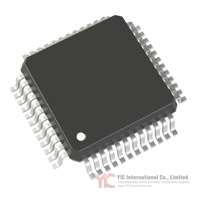
The S32K118 is available in multiple package options including 32-pin QFN, 48-pin LQFP, 64-pin LQFP, 100-pin LQFP, 100-pin MAPBGA, 144-pin LQFP, and 176-pin LQFP configurations. The 48-pin LQFP package, specified for the FS32K118LAT0MLFT variant, provides a balance between pin count and board space requirements, suitable for moderate-complexity applications.

All devices within a common package are pin-to-pin compatible, enabling design flexibility and potential migration to higher-pin-count variants if application requirements expand. Package selection depends on peripheral requirements, with higher pin counts providing access to additional communication interfaces and I/O functions.

Proper PCB layout following NXP design guidelines ensures optimal device performance. Decoupling capacitors must be placed close to power pins, with recommended values of 10 µF, 0.1 µF, and 1 nF in parallel to filter noise across multiple frequency ranges. Ground planes and proper trace routing minimize impedance and reduce electromagnetic interference.

Conclusion

The S32K118 microcontroller delivers a comprehensive embedded processing solution combining ARM Cortex-M0+ performance with extensive peripheral integration and power management flexibility. The 256 KB flash memory, multiple communication interfaces, and analog signal processing capabilities address requirements across industrial control, automotive, and consumer applications. Robust security features, comprehensive debug support, and wide operating temperature range enable deployment in demanding environments. The device's flexible power management modes and low-power operation support battery-powered and energy-constrained applications. Multiple package options and pin-compatible variants provide design scalability as application requirements evolve.

Frequently Asked Questions (FAQ)

Q1. What is the maximum operating frequency of the S32K118, and how does it affect power consumption?
A1. The S32K118 operates at up to 48 MHz in standard RUN mode. Higher frequencies increase power consumption proportionally, as dynamic power dissipation scales with clock frequency. Applications can reduce power consumption by operating at lower frequencies when full performance is not required, or by transitioning to lower-power modes during idle periods. The device supports dynamic frequency scaling, allowing runtime adjustment of clock frequency based on workload demands.
Q2. How much flash memory does the S32K118 provide, and is it sufficient for typical embedded applications?
A2. The S32K118 provides 256 KB of program flash memory with ECC protection. This capacity accommodates moderately complex firmware including real-time operating systems, application logic, and data tables. For applications requiring larger code footprints, higher-capacity variants within the S32K family offer up to 2 MB of flash memory. The 64 KB FlexNVM provides additional data storage for configuration parameters and operational logs.
Q3. What communication interfaces does the S32K118 support for connecting to external devices?
A3. The S32K118 integrates three LPUART modules for serial communication, three LPSPI modules for synchronous serial interfaces, two LPI2C modules for two-wire communication, and three FlexCAN modules for CAN bus networking. A FlexIO module enables software implementation of additional protocols. This comprehensive interface set supports connectivity to sensors, displays, memory devices, and network nodes in embedded systems.
Q4. How does the S32K118 protect against power supply variations and voltage transients?
A4. The S32K118 includes Low Voltage Reset (LVR), Low Voltage Detect (LVD), and Power-On Reset (POR) circuits that monitor supply voltage and trigger automatic resets if voltage drops below safe operating thresholds. The device operates across a 2.7 V to 5.5 V supply range, accommodating both 3.3 V and 5.0 V systems. Proper decoupling capacitors on power pins filter high-frequency noise and stabilize supply voltage during transient current demands.
Q5. What power management modes are available in the S32K118, and when should each be used?
A5. The S32K118 provides RUN mode for active processing at full frequency, VLPR mode for reduced-power background tasks, STOP mode for rapid wake-up from idle states, and VLPS mode for extended low-power operation. RUN mode is used during active processing. VLPR mode suits applications requiring occasional processing with minimal power consumption. STOP mode enables rapid response to interrupts while reducing idle power. VLPS mode minimizes power consumption during extended idle periods where occasional wake-up events are acceptable.
Q6. How does the ADC in the S32K118 perform with noisy analog signals?
A6. The S32K118 ADC includes hardware averaging capability that accumulates multiple conversions to reduce noise effects. Programmable averaging from 4 to 32 samples improves signal-to-noise ratio for noisy inputs. External filtering with capacitors on analog input pins further reduces high-frequency noise. Proper PCB layout with separate analog and digital ground planes minimizes coupling of digital switching noise into analog signal paths. The comparator's programmable hysteresis prevents false triggering from signals near comparison thresholds.
Q7. What security features does the S32K118 provide for protecting sensitive data?
A7. The S32K118 includes a Cryptographic Services Engine (CSEc) implementing hardware-accelerated encryption and decryption functions per the Secure Hardware Extension specification. Each device has a unique 128-bit identification number for device-specific authentication. Error-Correcting Code (ECC) on flash and SRAM detects and corrects single-bit errors. The System Memory Protection Unit prevents unauthorized access to protected memory regions. These features collectively enable secure data storage and communication in connected applications.
Q8. How does the S32K118 support real-time control applications requiring precise timing?
A8. The S32K118 provides eight independent 16-bit FlexTimer modules with up to eight channels each for input capture, output compare, and PWM generation. These timers operate at system clock frequency, enabling nanosecond-level timing precision. Two Programmable Delay Blocks coordinate ADC sampling with external events. A 32-bit Real Time Counter maintains time-of-day information. The configurable NVIC prioritizes interrupt handling for time-sensitive events. This comprehensive timing infrastructure supports motor control, power conversion, and synchronized multi-channel applications.
Q9. What package options are available for the S32K118, and how do they affect design flexibility?
A9. The S32K118 is available in 32-pin QFN, 48-pin LQFP, 64-pin LQFP, 100-pin LQFP, 100-pin MAPBGA, 144-pin LQFP, and 176-pin LQFP packages. The 48-pin LQFP variant balances pin count and board space for moderate-complexity applications. Higher pin-count packages provide access to additional communication interfaces and I/O functions. All devices within a common package are pin-to-pin compatible, enabling migration to higher-capacity variants if application requirements expand without redesigning the PCB.
Q10. How should the S32K118 be decoupled on the PCB to ensure stable operation?
A10. Decoupling capacitors must be placed as close as possible to power pins, with recommended values of 10 µF, 0.1 µF, and 1 nF in parallel to filter noise across multiple frequency ranges. All capacitors should be low-ESR ceramic types (X7R). Trace lengths from capacitors to pins should not exceed 2 mm. Ground connections should be as short as possible to the ground plane beneath the device. Separate analog and digital ground planes with a single connection point minimize coupling of digital switching noise into analog circuits. Following these practices ensures power supply stability and optimal device performance.
Q11. What is the typical power consumption of the S32K118 in different operating modes?
A11. Power consumption varies significantly with operating mode and frequency. In RUN mode at 48 MHz with peripherals disabled, typical consumption is approximately 15-20 mA. VLPR mode reduces consumption to 2-5 mA with limited functionality. STOP mode consumes 100-500 µA depending on peripheral retention requirements. VLPS mode achieves ultra-low consumption below 100 µA. Actual consumption depends on specific peripheral usage, clock frequency, and silicon process variation. Developers should measure power consumption in their specific application configuration for accurate power budget calculations.
Q12. How does the S32K118 support debugging during firmware development?
A12. The S32K118 integrates a Serial Wire JTAG Debug Port supporting both SWD and JTAG interfaces for connection to development tools. The Debug Watchpoint and Trace module enables non-intrusive breakpoint setting and data watchpoint monitoring. The Instrumentation Trace Macrocell captures real-time program execution flow for performance analysis. The Flash Patch and Breakpoint Unit enables software breakpoints without modifying flash memory. These features support rapid firmware development, debugging, and optimization workflows from initial development through production testing.
Slide the scroll wheel to view more.
Click to see more

User Review

  • Kent***orimoto

    Used this processor in a wireless networking project. Stable operation and good integration with existing software tools. Performance is sufficient for embedded communication applications.

    June 9th, 2026

  • Oliv***ughes

    Good capacitor quality. Used in a power supply rebuild and measured values were close to spec. No issues after several days of continuous operation.

    June 5th, 2026

  • Kevi***rner

    Very good MCU for legacy embedded projects. I used the LPC2387FBD100 in an industrial control board replacement and it integrated more smoothly than expected. Ethernet and peripheral support were enough for our needs. Been running continuously for over a week without instability.

    May 25th, 2026

  • Nath***ill

    Good supervisor IC for automotive power systems. Reliable reset behavior.

    May 19th, 2026

  • Jack***III

    Good price

    May 15th, 2026

  • Davi***ung

    Good SoC for networking applications. Stable signal processing and low power consumption.

    May 6th, 2026

  • Andr***ee

    Overall is good

    April 28th, 2026

  • Emil***ark

    Accurate frequency output for timing circuits. Works well in low-power signal designs.

    April 23th, 2026

  • Jose***Dong

    Quick response and clear answers.

    April 16th, 2026

  • Marc***echLab

    Excellent quality. All chips passed testing and showed consistent electrical characteristics.

    April 7th, 2026

  • Circ***MasterX

    Good packaging and fast shipping. Performance is stable, but I wish there was clearer labeling on each component.

    April 2th, 2026

  • SamT***Reviews

    Excellent ICs. Used them in a communication module and performance was stable.

    March 27th, 2026

  • Kevi***.

    Good quality parts. No failures during testing.

    March 17th, 2026

  • Bria***.

    Good

    March 13th, 2026

  • Mari***.

    Superb performance.

    March 2th, 2026

  • Emma***

    Excellent ICs for DIY projects. Came well-packaged, genuine parts, and all tested good on my bench. No fails on 50 pieces.

    February 26th, 2026

  • Gadg***an123

    Good

    February 10th, 2026

  • Quan***PartsLab

    Great service

    February 6th, 2026

  • Vect***upplyChain

    The sales rep was professional and responsive.

    January 27th, 2026

  • Puls***vePurchasing

    Components were packed carefully with anti-static protection and cushioning. Everything arrived in good condition.

    January 23th, 2026

  • Pixe***ocure

    Components were packed well. Appreciated the attention to detail.

    January 13th, 2026

  • Byte***dgeBuyer

    Good Quality & Fast Response

    January 5th, 2026

  • Circ***AtlasGlobal

    JUST WHAT I WANT

    December 30th, 2025

  • Allo***taImports

    Very professional

    December 26th, 2025

  • Apex***i

    Quick response and prompt shipping

    December 19th, 2025

  • Hexa***e Circuits

    We were surprised by how quickly our order was processed. From inquiry to delivery, everything was smooth. A trustworthy IC distributor with good stock levels.

    December 11th, 2025

  • Core***se Inc.

    Good customer service

    December 2th, 2025

  • Skyl***Drew

    Delivered ahead of schedule.

    November 28th, 2025

  • Byte***ad

    We purchased a batch of XC6SLX25T-2CSG324C from yic-electronics. Clean markings, fresh 2024 date codes, and antistatic packaging—service was efficient and polite.

    November 17th, 2025

  • avl_***rcing_julia

    Smooth checkout and same-day ship via FedEx. Parts arrived dry-packed, correct MSL labels, and fresh date codes.

    November 13th, 2025

  • Liam***hnson

    Price is good. Order processed quickly, and tracking provided the same night.

    November 3th, 2025

  • Yuko***kamura

    Prices were reasonable compared to other brokers. One reel had minor box damage, but the inner pack was intact.

    October 31th, 2025

  • Opti***

    Excellent prices and top-notch customer service. Even the standard shipping was surprisingly fast. Components were well-packed and genuine. Totally satisfied with the purchase.

    October 21th, 2025

  • Thom***Gray

    Clear communication and on-time delivery.

    October 15th, 2025

  • Aaro***ughes

    Excellent supplier. Great communication and reliable service throughout the process.

    October 9th, 2025

  • Auro***hip

    Good experience overall. The order was processed smoothly, packaging was secure, and the delivery time was acceptable.

    September 29th, 2025

  • Jimm***

    I had a great experience with this company. They were very professional and efficient, and they had the obsolete parts I needed in stock. Once payment was processed, the delivery was quick—my goods arrived within two weeks. The customer service was friendly professional, with seamless communication throughout. Overall, everything went smoothly, and I would definitely recommend them.

    September 19th, 2025

  • Jaso***in

    The purchase was easy and fast. Polite and helpful seller, great price.

    September 8th, 2025

  • NeoB***

    Schnelle Lieferung, Produkt entspricht der Beschreibung, hochwertige Verarbeitung, stabile Funktion, alles passt perfekt, sehr zufrieden mit dem Kauf.

    September 2th, 2025

  • Tobi***

    Quick response, good price and clear communication. Very satisfied with the service

    August 28th, 2025

  • Zóc***Nights

    Not bad

    August 19th, 2025

  • 3174***41@gmail.com

    Bought once to know that YIC electronic components quality is good, and the price is not expensive, very affordable, fast delivery!
    Really recommend buying electronic components here!

    April 14th, 2025

  • Yush***nagahata

    YIC is an excellent company.
    The deliverry time is fast, and we find it very usueful for procuring electronic components.
    We look forward to continuing our relationship in the future.
    Go YIC! Keep up the great work!

    February 20th, 2025

  • SAMI*** INSTALLATION

    Fantastic! Shure I would buy again with YIC

    January 23th, 2025

  • Aadh***x

    The experience with YIC International was great. They not only provided support for the proposed parts but also proactively suggested additional parts that could be useful for us. They have reviewed all the parts properly and corrected our requirements. The delivery and other logistical support were excellent.

    January 22th, 2025

  • Ke*

    A Reliable and Trustworthy Partner
    Received original, high-quality components with fast shipping from YIC electronics.

    November 25th, 2024

  • Nana***risnawan

    Great component supplier, a place that easy to find electronics parts at a good price and delivery.

    August 6th, 2024

  • Alge***n Gholson

    Great products, fast delivery.
    The quality and service of YIC Electronics' components are at the top of the industry. Highly recommended.

    February 20th, 2024

  • Frey***.

    Our partnership with YIC Electronics has been exceptionally satisfying. Their unwavering commitment to outstanding customer service, coupled with their highly competitive pricing and unwavering dedication to top-notch, high-performance product quality, has consistently impressed us. YIC Electronics stands out as a true industry leader in every aspect of their service. Their swift and efficient logistics feedback further underscores their professionalism and reliability.

    August 25th, 2023

  • Jo C***n

    High Quality Products!
    I received genuine, high-quality electronic parts. Thank you YIC electronics.

    August 12th, 2023

  • Edwa***W.

    Yic-electronics suppliers are top notch quality and consistent reliability, I have generated several orders from their website and their service has exceeded expectations in providing electronic components for our business needs.

    August 6th, 2023

  • Anna***

    Yic-electronics is a good partner for our company, we have been cooperating with each other for 4 years, and the cooperation is all smooth and there is no dispute about the goods. Our latest transaction with Yic-electronics happened a month ago, and the process was very smooth, thanks to Yic-electronics's help!

    June 17th, 2023

0 Articles

Post a Review

Hello , welcome to comment on this product
Rating *
5.0

Please limit the remark to 500 words

Your personal information will be hidden

FAQFrequently Asked Questions

  • When designing a compact automotive sensor module utilizing the FS32K118LAT0MLFT, what are the critical considerations for the 48-LQFP (7x7mm) package regarding PCB layout and thermal dissipation to prevent overheating, especially in a high-temperature automotive environment with limited airflow? For the FS32K118LAT0MLFT in its 48-LQFP (7x7mm) package, meticulous PCB layout is paramount. Ensure adequate copper pour on both sides of the PCB, particularly under the package, to act as a heatsink. Utilize thermal vias connecting the ground plane under the IC to other ground planes to improve heat spreading. Consider the proximity of heat-generating components and ensure sufficient clearance. For critical applications operating near the maximum ambient temperature of 125°C, a dedicated heatsink might be necessary, even with proper PCB layout, if the expected power dissipation exceeds the thermal resistance capabilities of the board alone. The FS32K118LAT0MLFT's thermal resistance junction-to-ambient (Rth_JA) will be a key parameter to analyze in your thermal simulation.
  • Given the FS32K118LAT0MLFT's 2.7V to 5.5V supply voltage range, how can designers ensure robust operation and protect the microcontroller from voltage transients common in automotive power rails, particularly when interfacing with systems that may have less stringent power conditioning? Designing for the FS32K118LAT0MLFT's wide supply range (2.7V to 5.5V) requires careful attention to power supply filtering and decoupling. Use a combination of bulk capacitors and high-frequency ceramic capacitors placed as close as possible to the VDD/VCC pins to mitigate noise. Implementing a robust voltage supervisor or brown-out detection circuit is highly recommended, especially if the 5.5V maximum is frequently approached, to prevent unintended resets or data corruption during voltage excursions. For automotive applications, consider transient voltage suppression (TVS) diodes on the power input to protect the FS32K118LAT0MLFT from automotive-specific voltage spikes.
  • The FS32K118LAT0MLFT features 256KB of FLASH program memory and 25K x 8 RAM. For a complex control application requiring significant data buffering and lookup tables, how can engineers effectively manage memory allocation and optimize code size to maximize the available resources without compromising performance or exceeding the program memory limit? Optimizing memory usage for the FS32K118LAT0MLFT involves a multi-pronged approach. Developers should utilize compiler optimization flags aggressively. Employing a linker script to tightly control section placement and memory mapping can be beneficial. For large datasets, consider storing them in external memory if absolutely necessary and the system design permits, though for the FS32K118LAT0MLFT, maximizing internal FLASH and RAM is preferred. Techniques like code profiling to identify and optimize performance-critical routines that consume significant code space, and data compression or efficient data structures for lookup tables, are essential for efficient use of the 256KB FLASH and 25K x 8 RAM of the FS32K118LAT0MLFT.
  • When migrating an existing design from a similar microcontroller to the FS32K118LAT0MLFT, what are the key differences in the ARM Cortex-M0+ core architecture and the peripheral set (e.g., CANbus, FlexIO, LINbus, SPI, UART) that an engineer must be aware of to avoid compatibility issues and ensure a smooth transition? Transitioning to the FS32K118LAT0MLFT requires understanding the nuances of its ARM Cortex-M0+ core, which is a lower-power, efficiency-focused architecture compared to some higher-end ARM cores. While instruction sets are largely compatible, subtle differences in interrupt handling or low-power modes might necessitate code adjustments. Critically, the FlexIO module on the FS32K118LAT0MLFT offers programmable I/O capabilities, providing flexibility but requiring a different configuration approach than dedicated peripheral interfaces found on other MCUs. Thoroughly review the peripheral reference manuals for CANbus, FlexIO, LINbus, SPI, and UART on the FS32K118LAT0MLFT to understand their specific register sets, operational modes, and potential behavioral differences from your previous microcontroller.
  • For an automotive infotainment system requiring reliable communication over CANbus and LINbus, what potential challenges or design considerations arise when implementing these protocols on the FS32K118LAT0MLFT, particularly concerning interrupt latency and timing precision? Implementing CANbus and LINbus on the FS32K118LAT0MLFT demands attention to interrupt latency and timing precision. The ARM Cortex-M0+ core, while efficient, may have slightly higher interrupt latency than higher-performance cores. This can impact the ability to meet stringent real-time deadlines for certain CANbus messages or LINbus frames. Developers should carefully analyze the interrupt priorities and service routine execution times. Utilizing DMA for efficient data transfer to and from the CAN and LIN peripherals can significantly offload the CPU and improve throughput and timing accuracy. Testing under worst-case bus load conditions is crucial to validate the FS32K118LAT0MLFT's suitability for your specific communication requirements.
  • With the FS32K118LAT0MLFT having 43 I/O pins, and a requirement for a mix of digital inputs, outputs, and analog signals for sensor interfacing, how can engineers effectively plan the pinout to accommodate all necessary peripherals while minimizing signal contention and ensuring sufficient driving strength for external components? Pinout planning for the FS32K118LAT0MLFT's 43 I/O pins is a critical step. The product specification lists CANbus, FlexIO, SPI, and UART, along with analog-to-digital converter (A/D) inputs. Developers must map these functions strategically. For instance, shared pins between analog and digital functions will require careful configuration in software to switch modes. Consider the drive strength requirements of external components; if driving LEDs or relays, ensure the chosen pins can supply adequate current, or use external buffer ICs. Furthermore, routing critical high-speed signals like SPI or CANbus away from noisy digital signals can prevent interference. Reviewing the FS32K118LAT0MLFT's multiplexing capabilities for each pin is essential to maximize flexibility.
  • In applications where the FS32K118LAT0MLFT operates at its lower supply voltage of 2.7V, how do the performance characteristics of the internal oscillator and the ADC converters (16x12b SAR) change, and what steps can be taken to ensure adequate signal integrity and measurement accuracy? At the lower end of its operating voltage range (2.7V), the FS32K118LAT0MLFT's internal oscillator may exhibit slightly reduced frequency stability, although it's generally designed to operate within its specified frequency across the entire voltage range. More critically, the performance of the 16x12b SAR ADC can be affected by lower supply voltages. Reduced signal-to-noise ratio (SNR) and a potentially smaller effective number of bits (ENOB) could occur. To mitigate this, ensure that analog input signals are well-conditioned, with minimal noise. Employing software averaging or oversampling techniques on the ADC readings from the FS32K118LAT0MLFT can improve the effective resolution and accuracy. Careful calibration of the ADC at the intended operating voltage is also advisable.
  • What are the long-term availability and potential obsolescence concerns for the FS32K118LAT0MLFT, especially for projects with extended lifecycles in the automotive or industrial sectors, given its current quantity and RoHS compliance status? For projects with extended lifecycles, understanding the long-term availability of the FS32K118LAT0MLFT is crucial. While the current quantity of 1215 units suggests a healthy stock, it’s imperative to engage with NXP Semiconductors or authorized distributors regarding their product lifecycle management and End-of-Life (EOL) policies for the FS32K118 family. RoHS compliance indicates adherence to current environmental regulations, which is positive. However, proactive communication with NXP regarding their forecast for the FS32K118LAT0MLFT is the best approach to mitigate obsolescence risks and ensure a sustained supply chain for your application.
  • When developing for safety-critical applications with the FS32K118LAT0MLFT, what specific certification standards (e.g., ISO 26262 automotive functional safety) should engineers consider, and what evidence or design practices are typically required to demonstrate compliance for a microcontroller of this class? For safety-critical applications, particularly in automotive where ISO 26262 is prevalent, the FS32K118LAT0MLFT would be evaluated based on its suitability for specific Automotive Safety Integrity Levels (ASILs). NXP typically provides safety documentation, such as FMEDA (Failure Modes, Effects, and Diagnostic Analysis) reports, for their automotive-grade microcontrollers. Engineers must ensure their design implementation also adheres to functional safety principles, including robust error detection mechanisms, redundancy where necessary, and comprehensive testing. The presence of peripherals like WDT (Watchdog Timer) on the FS32K118LAT0MLFT is a foundational element for safety, but demonstrating compliance involves a holistic approach covering hardware, software, and development processes.
  • For applications requiring flexible and efficient handling of multiple serial communication protocols simultaneously, how does the FS32K118LAT0MLFT's FlexIO peripheral compare to traditional dedicated UART or SPI interfaces in terms of configurability, performance, and potential complexity in software development? The FlexIO peripheral on the FS32K118LAT0MLFT offers significantly higher flexibility than traditional dedicated UART or SPI interfaces. It allows designers to emulate various serial protocols, including SPI, UART, I2C, and even custom protocols, using a highly configurable set of hardware shifters and timers. This can be advantageous when protocol requirements evolve or when interfacing with non-standard devices. However, this flexibility comes with increased software complexity. Configuring the FlexIO peripheral for the FS32K118LAT0MLFT requires a deeper understanding of its internal state machines and shift/timer configurations compared to simply setting up registers for a standard UART or SPI. For straightforward, high-volume applications, dedicated peripherals might be simpler, but for intricate communication needs or space-constrained designs requiring protocol consolidation, FlexIO on the FS32K118LAT0MLFT is a powerful option.
  • How can the DMA controller integrated into the FS32K118LAT0MLFT be leveraged to offload CPU intensive tasks, such as transferring data between memory and peripherals like CANbus or the ADC, to improve overall system responsiveness and power efficiency in a battery-powered application? The Direct Memory Access (DMA) controller on the FS32K118LAT0MLFT is a key enabler for improving system performance and power efficiency. By configuring DMA channels to transfer data directly between peripherals (e.g., CANbus receiving buffers, ADC data registers) and memory, the CPU is freed from performing byte-by-byte transfers. This significantly reduces CPU load, allowing it to enter lower power states or dedicate more cycles to critical control algorithms. For instance, continuous ADC sampling for monitoring an analog sensor can be handled entirely by DMA, with the CPU only being interrupted when a buffer is full or a specific condition is met. Effectively utilizing the DMA for data movement with the FS32K118LAT0MLFT is crucial for optimizing both throughput and energy consumption.
  • When designing with the FS32K118LAT0MLFT for an application requiring precise timing for PWM generation, what factors influence the accuracy and resolution of the PWM outputs, and are there specific considerations when using the FlexIO for PWM compared to dedicated PWM timers? The accuracy and resolution of PWM outputs from the FS32K118LAT0MLFT are primarily determined by the clock source frequency feeding the PWM generation logic and the bit-width of the counter used. For dedicated PWM timers, you'll configure the timer period and duty cycle registers. If using the FlexIO for PWM generation, the underlying hardware shifters and timers are configured to mimic PWM behavior. While FlexIO can offer very fine-grained control, the complexity of setting up the correct sequences for precise duty cycle control might be higher. Developers should carefully analyze the clocking scheme for the PWM module or FlexIO timers on the FS32K118LAT0MLFT and understand how the resolution is achieved (e.g., 8-bit, 10-bit, 12-bit) to meet the specific timing requirements of their application.
  • What are the implications of using the FS32K118LAT0MLFT's internal oscillator versus an external crystal oscillator for timing-critical applications such as high-speed SPI communication or precise motor control, particularly concerning frequency drift and jitter? For timing-critical applications on the FS32K118LAT0MLFT, the choice between its internal oscillator and an external crystal oscillator has significant implications. The internal oscillator, while convenient and space-saving, generally has lower accuracy and stability, with higher susceptibility to temperature and voltage variations. This can lead to frequency drift and jitter, which can negatively impact high-speed SPI data integrity or the precision of motor control PWM signals. An external crystal oscillator, when properly implemented with load capacitors, provides a much more stable and accurate reference frequency, minimizing drift and jitter, thus ensuring more reliable operation for demanding timing requirements of the FS32K118LAT0MLFT.
  • The FS32K118LAT0MLFT offers 2K x 8 of EEPROM. What are the typical use cases for this non-volatile memory in embedded systems, and what are the considerations for wear leveling and data retention when storing frequently updated calibration parameters or configuration settings? The 2K x 8 EEPROM on the FS32K118LAT0MLFT is typically used for storing non-volatile data that needs to persist across power cycles. This commonly includes calibration data, configuration parameters, unique device identifiers, or fault logs. When storing frequently updated parameters, wear leveling becomes a critical consideration. Standard EEPROM cells have a limited number of write/erase cycles (typically in the tens or hundreds of thousands). Without wear leveling techniques (e.g., distributing writes across different memory locations or using a shadow copy), premature wear-out of the EEPROM can occur. Data retention is also a factor; while EEPROM offers good retention (often 10-20 years), the integrity of stored data over the product's lifetime should be considered, especially for critical configuration settings of the FS32K118LAT0MLFT.
  • For a product designed to operate in harsh electromagnetic interference (EMI) environments, what specific design guidelines should be followed when integrating the FS32K118LAT0MLFT and its associated components to minimize susceptibility and radiated emissions? To minimize EMI susceptibility and radiated emissions when integrating the FS32K118LAT0MLFT, a comprehensive approach is necessary. Implement robust decoupling for all power and ground pins. Route critical high-speed signals (SPI, CANbus, UART) with controlled impedance and keep them as short as possible. Use ground planes effectively to provide a low-impedance return path for signals. Consider shielding for the entire PCB or specific sensitive components if necessary. Filtering of external interfaces is also crucial, particularly for I/O pins that connect to the outside world. Minimizing clock jitter and using spread-spectrum clocking, if supported and applicable to the FS32K118LAT0MLFT's clocking options, can also help reduce radiated emissions.
  • In a scenario where the FS32K118LAT0MLFT is used in a system that experiences power loss events, how does the WDT (Watchdog Timer) function contribute to system recovery, and what are the best practices for configuring its timeout period to reliably detect and recover from software hangs without causing spurious resets? The Watchdog Timer (WDT) on the FS32K118LAT0MLFT acts as a critical safety mechanism to prevent system lock-ups. If the main application software fails to periodically "kick" or reset the WDT before its timeout period expires, the WDT will trigger a system reset. This is essential for recovering from software hangs caused by errors or unexpected conditions. For optimal configuration, the WDT timeout period should be set longer than the longest expected normal execution path of the application but shorter than the maximum tolerable time for an unresponsive system. Debugging the application's execution flow to determine appropriate WDT timings for the FS32K118LAT0MLFT is crucial to avoid false triggers while ensuring timely recovery from genuine hangs.
  • When considering alternative microcontrollers for an application currently using the FS32K118LAT0MLFT, what are the key architectural features and peripheral sets to look for in pin-compatible or functionally equivalent devices that offer advantages in terms of processing power, memory, or advanced communication interfaces? When evaluating alternatives to the FS32K118LAT0MLFT, focus on microcontrollers within the NXP S32K family or other ARM Cortex-M0+ or Cortex-M4 based devices. Key features to compare include higher clock speeds (e.g., >48MHz), increased FLASH and RAM capacity (e.g., >256KB FLASH, >25KB RAM), additional or enhanced communication peripherals like more robust CAN controllers, Ethernet MAC, or USB, and potentially more advanced analog-to-digital converters or digital-to-analog converters. If pin compatibility is a strict requirement, the search will be more constrained. However, functional equivalence allows for PCB redesign and potentially offers access to newer technologies or better cost-performance ratios.
  • How can the integrated data converters (16x12b SAR ADC and 1x8b DAC) on the FS32K118LAT0MLFT be utilized for complex analog signal processing tasks, such as implementing a basic control loop or performing spectrum analysis, within the constraints of its clock speed and processing capabilities? The 16x12b SAR ADC on the FS32K118LAT0MLFT is capable of providing sufficient resolution for many analog signal processing tasks. By carefully selecting sampling rates, using DMA for efficient data acquisition, and leveraging the ARM Cortex-M0+ core, engineers can implement control loops or basic spectrum analysis. For example, a PID control loop can be implemented by reading sensor values via the ADC, performing calculations, and then adjusting outputs via PWM or the 1x8b DAC. For spectrum analysis, techniques like the Fast Fourier Transform (FFT) can be implemented, though the computational complexity will be limited by the 48MHz clock speed and available RAM on the FS32K118LAT0MLFT. The 1x8b DAC can be used for generating simple analog reference signals or for basic audio output.
  • What are the critical aspects of the 48-LQFP (7x7mm) package type for the FS32K118LAT0MLFT when considering automated assembly and rework processes in a high-volume manufacturing environment? The 48-LQFP (7x7mm) package for the FS32K118LAT0MLFT presents specific considerations for automated assembly. Its relatively small size and fine pitch require precise pick-and-place equipment for accurate placement. Solder paste application and reflow soldering profiles must be carefully optimized to ensure good solder joint formation and prevent bridging or voids, especially under the package with its exposed pad. Reworking LQFP packages can be challenging due to their lead structure and thermal sensitivity; specialized hot air or infrared rework stations are typically required, and a high success rate depends on proper board design with adequate clearances and robust solder joint design for the FS32K118LAT0MLFT.
  • Given the FS32K118LAT0MLFT's RoHS 3 compliance, what implications does this have for the selection of other components in the bill of materials, particularly concerning lead-free solder alloys and potential compatibility issues with older leaded components? RoHS 3 compliance for the FS32K118LAT0MLFT means it meets stringent regulations on hazardous substances, including lead. This mandates the use of lead-free solder alloys (typically tin-silver-copper, SAC alloys) in the manufacturing process. When selecting other components for the bill of materials, ensure they are also RoHS 3 compliant and rated for lead-free assembly temperatures, as these can be higher than those used for traditional tin-lead solder. Mixing leaded and lead-free components or using components not rated for lead-free processes can lead to poor solder joint reliability, increased defect rates, and potential manufacturing challenges for your product utilizing the FS32K118LAT0MLFT.