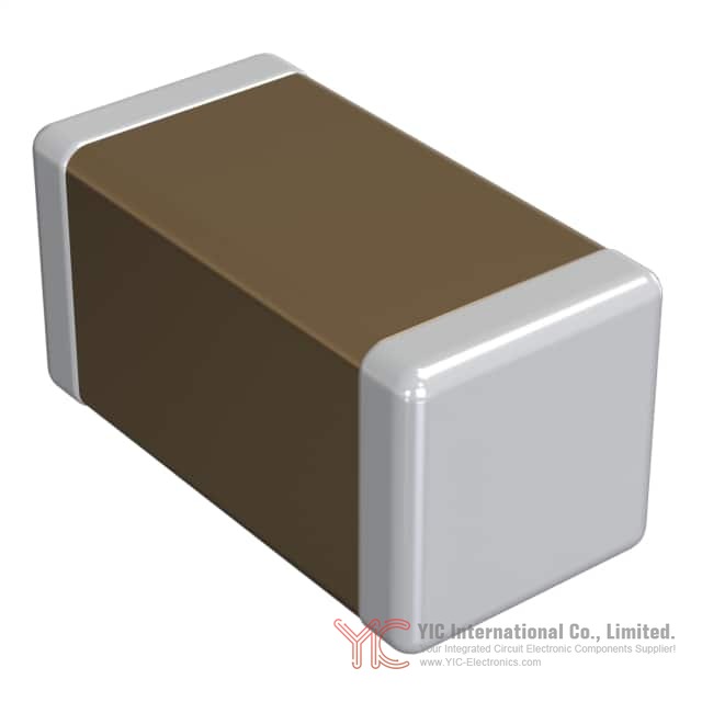
Product Overview of the GQM1875C2E2R4CB12D Series
The Murata GQM1875C2E2R4CB12D is a high-Q multilayer ceramic capacitor designed for general-purpose electronic equipment requiring voltage ratings above 100V DC. This 2.4 pF capacitor with ±0.25 pF tolerance operates at 250V DC, making it suitable for applications demanding both precision and reliability in high-voltage environments. The device employs C0G (NP0) dielectric material, which provides stable capacitance across temperature and voltage variations—a characteristic that distinguishes it from high-dielectric-constant alternatives.
The 0603 package format (1608 metric) represents a standard surface-mount configuration that balances component density with handling practicality. The GQM1875C2E2R4CB12D series represents Murata's commitment to delivering components that maintain performance integrity under demanding operational conditions while accommodating modern manufacturing processes.
Electrical Specifications and Performance Characteristics of the GQM1875C2E2R4CB12D
The GQM1875C2E2R4CB12D delivers a nominal capacitance of 2.4 pF with a tolerance band of ±0.25 pF, providing the precision necessary for frequency-determining circuits and impedance matching applications. The rated voltage of 250V DC establishes the maximum continuous voltage that can be safely applied across the device terminals without risk of dielectric breakdown.
Measurement of capacitance for the GQM1875C2E2R4CB12D must occur at the voltage and frequency specified in the product documentation. The high-Q characteristic of this series indicates low dielectric loss, translating to minimal energy dissipation during operation. This property becomes particularly valuable in RF and high-frequency applications where signal integrity depends on component efficiency.
The C0G dielectric material used in the GQM1875C2E2R4CB12D exhibits minimal capacitance change across the operating temperature range, distinguishing it from high-dielectric-constant alternatives that experience more pronounced variations. This stability makes the GQM1875C2E2R4CB12D suitable for time-constant circuits and precision filtering applications where capacitance tolerance must remain tight throughout the product lifecycle.
Temperature Behavior and Capacitance Stability in the GQM1875C2E2R4CB12D
The electrical characteristics of the GQM1875C2E2R4CB12D change with temperature, though the C0G dielectric formulation minimizes these variations compared to other ceramic capacitor types. When designing circuits using the GQM1875C2E2R4CB12D, engineers should select a capacitance value appropriate for the intended operating temperature range rather than relying on room-temperature specifications alone.
The capacitance of the GQM1875C2E2R4CB12D may shift within the rated temperature window, necessitating careful evaluation during circuit design. For applications requiring narrow capacitance tolerance—such as oscillator circuits or precision timing networks—designers must account for temperature-induced shifts and confirm performance under actual system conditions before production deployment.
The GQM1875C2E2R4CB12D exhibits aging characteristics whereby capacitance decreases gradually over time. This aging effect, while modest in C0G materials, should be considered in long-term reliability assessments. Designers working with the GQM1875C2E2R4CB12D in applications sensitive to capacitance drift should evaluate aging behavior using actual equipment operating at intended environmental conditions.
Voltage Operating Conditions for the GQM1875C2E2R4CB12D
The 250V DC rating of the GQM1875C2E2R4CB12D establishes the absolute maximum continuous voltage between terminals. Applied voltage must never exceed this rated value, as overvoltage conditions can trigger dielectric breakdown and catastrophic failure. When AC voltage is superimposed on DC voltage in circuits using the GQM1875C2E2R4CB12D, the zero-to-peak voltage must remain below the 250V rating. Similarly, when AC or pulse voltage is applied alone, the peak-to-peak voltage cannot exceed 250V.
Abnormal voltage conditions—including surge voltage, static electricity, and pulse transients—must also remain within the 250V limit. Exceeding this threshold may cause electrical short circuits through breakdown of internal dielectric layers. The time to failure under overvoltage conditions depends on both the applied voltage magnitude and ambient temperature, with higher temperatures accelerating breakdown.
The GQM1875C2E2R4CB12D should not be used in AC voltage circuits or pulse voltage circuits without careful evaluation of self-heating effects. When AC or pulse current flows through the device, dielectric losses generate heat. The surface temperature of the GQM1875C2E2R4CB12D, including temperature rise from self-heating, must remain within the maximum operating temperature limit. As a design guideline, self-heating should be limited to 20°C above ambient temperature (measured at 25°C ambient) to maintain long-term reliability.
Physical Dimensions and Packaging of the GQM1875C2E2R4CB12D
The GQM1875C2E2R4CB12D employs a 0603 package format with metric dimensions of 1.6mm × 0.8mm, representing a compact surface-mount configuration suitable for high-density PCB layouts. The device arrives in tape-and-reel packaging designed for automated assembly processes, with standard reel dimensions and taping specifications that ensure compatibility with pick-and-place equipment.
The GQM1875C2E2R4CB12D is supplied on carrier tape with controlled pitch spacing of 40 ± 0.3 mm (accumulate pitch of 10 sprocket holes). The top and bottom tapes enclosing the component maintain minimum breakdown forces of 5N, ensuring secure retention during transport and handling. Peeling force for tape removal ranges from 0.1N to 0.6N, providing controlled separation without component damage.
Reel construction for the GQM1875C2E2R4CB12D uses resin materials with dimensions specified to accommodate standard feeder systems. Labels on the reel exterior identify the customer part number, manufacturer part number, company name, inspection number, and quantity, facilitating inventory management and traceability throughout the supply chain.
Storage Requirements and Environmental Conditions for the GQM1875C2E2R4CB12D
Proper storage conditions directly influence the performance and reliability of the GQM1875C2E2R4CB12D. The device should be maintained at room temperature between 5°C and 40°C with relative humidity between 20% and 70%. High-temperature and high-humidity storage conditions, or prolonged storage periods, can degrade packaging materials and promote electrode oxidation.
If more than six months have elapsed since delivery of the GQM1875C2E2R4CB12D, visual inspection of packaging and mounting surfaces should occur before use. After one year of storage, solderability testing becomes necessary to confirm that oxidation has not compromised termination quality. The GQM1875C2E2R4CB12D should never be stored in atmospheres containing corrosive gases such as hydrogen sulfide, sulfur dioxide, chlorine, or ammonia, as these substances react with termination electrodes and degrade solderability.
Direct sunlight exposure and rapid humidity changes must be avoided during storage of the GQM1875C2E2R4CB12D, as photochemical changes and moisture condensation can deteriorate both solderability and electrical performance. Maintaining stable environmental conditions throughout the storage period preserves the device's manufacturing quality and ensures consistent performance upon assembly.
Soldering and Assembly Processes for the GQM1875C2E2R4CB12D
Reflow soldering represents the primary assembly method for the GQM1875C2E2R4CB12D in modern manufacturing environments. The process requires careful temperature management to prevent mechanical damage from thermal shock. Preheating of both the GQM1875C2E2R4CB12D and PCB is mandatory, with temperature differential (ΔT) between solder and component surface kept as small as possible to minimize internal deformation.
For the GQM1875C2E2R4CB12D, lead-free solder composition of Sn-3.0Ag-0.5Cu is specified. Peak reflow temperature must be achieved to ensure proper solder wetting and joint formation. Insufficient reflow temperature can result in poor solder wettability, voids within solder joints, potential whiskering, reduced bonding strength, and loss of self-alignment properties. Tombstoning and component shifting on land patterns may also occur if reflow temperature falls below manufacturer specifications.
The GQM1875C2E2R4CB12D can also be assembled using flow soldering for certain package sizes (1.6×0.8mm to 2.0×1.25mm). Flow soldering requires similar preheating protocols and temperature differential management. Excessively long soldering time or high temperature can cause leaching of terminations, resulting in poor adhesion and capacitance loss through loss of contact between internal electrodes and external terminations.
Solder paste application for the GQM1875C2E2R4CB12D must be optimized to prevent both excess and insufficient solder. Overly thick solder paste creates excessive fillet height, increasing mechanical and thermal stress on the component and promoting cracking. Conversely, insufficient solder paste results in inadequate adhesive strength, potentially causing the GQM1875C2E2R4CB12D to separate from the PCB during subsequent handling or thermal cycling.
Flux selection for the GQM1875C2E2R4CB12D assembly should prioritize halide content below 0.1% maximum to prevent corrosion of terminations. Strong acidic flux can corrode the device and degrade performance, necessitating quality verification after mounting. Flux application should be thin and even to avoid excessive gas generation that compromises solderability.
Post-reflow correction of the GQM1875C2E2R4CB12D using a soldering iron requires preheating to specified temperature ranges to minimize thermal shock. Correction should be performed quickly to prevent solder leaching on terminal electrodes. A soldering iron tip of 3mm diameter or smaller is recommended, with solder wire diameter of 0.5mm or smaller. Spot heater correction offers advantages over soldering iron methods by distributing heat more evenly across the component and PCB, reducing thermal shock risk.
PCB Design Considerations for the GQM1875C2E2R4CB12D
Land pattern design significantly influences the reliability and performance of the GQM1875C2E2R4CB12D during assembly and field operation. Unlike leaded components, the GQM1875C2E2R4CB12D is mounted directly on the substrate and experiences greater susceptibility to flexing stresses. Excess solder fillet height multiplies mechanical and thermal stresses, potentially causing chip cracking.
Land dimensions for the GQM1875C2E2R4CB12D must be carefully selected based on the intended soldering method. For reflow soldering, specific land dimensions optimize solder joint formation while minimizing stress concentration. For flow soldering applications, land dimensions differ to accommodate the soldering process characteristics. Designers should evaluate actual PCB and assembly equipment to confirm suitable land dimensions before production implementation.
The thermal expansion coefficient mismatch between the GQM1875C2E2R4CB12D and PCB material can cause cracking due to differential expansion and contraction during thermal cycling. When the PCB material exhibits significantly different thermal expansion characteristics—particularly with fluorine resin boards or single-layer glass epoxy substrates—the risk of component cracking increases substantially. Material selection and board design should account for these thermal compatibility factors.
When replacing the GQM1875C2E2R4CB12D with smaller capacitors, designers must consider not only land size changes but also wiring width, wiring direction, and copper foil thickness. Simple land size reduction without comprehensive design review increases cracking risk. PCB expansion and contraction with temperature creates stress on the GQM1875C2E2R4CB12D that varies depending on PCB material and structure, requiring holistic design evaluation.
Mechanical Stress Management During Manufacturing of the GQM1875C2E2R4CB12D
Mounting position and orientation of the GQM1875C2E2R4CB12D on the PCB should minimize stress during board flexing or bending. Horizontal orientation of the component relative to the direction of applied stress reduces stress concentration. Positioning the GQM1875C2E2R4CB12D away from board separation points and screw holes further reduces mechanical loading during manufacturing and assembly operations.
Pick-and-place equipment must be properly maintained to prevent excessive forces on the GQM1875C2E2R4CB12D during mounting. The suction nozzle lowest position should be adjusted to prevent PCB bending. Accumulated dirt and dust in suction mechanisms create excessive force during placement, causing chip cracking. Worn locating claws impose uneven forces on components, necessitating periodic maintenance, inspection, and replacement of these critical equipment components.
Vibration and shock during manufacturing must be carefully controlled. Mechanical shock from dropping can cause internal dielectric cracking, compromising quality and reliability. When PCBs are stacked or handled, corner impacts from adjacent boards must be prevented to avoid component damage. Resonance generation during vibration exposure should be eliminated through proper mounting techniques and equipment setup.
Board separation and cropping operations present significant risk to the GQM1875C2E2R4CB12D if not properly executed. Bending and twisting stresses during cropping can crack the component, leading to insulation resistance degradation and potential short circuits. Router-type separators are preferred as they eliminate board bending during cutting. When disc separators are used, precise alignment of top and bottom blades, proper V-groove design, and careful depth control are essential to prevent board deflection stress.
For single-sided mounting, board separation jigs should hold the portion close to the jig and bend toward the component-mounted side to minimize stress. Double-sided mounting requires additional measures including component orientation parallel to the separation surface, strategic placement of slits near separation points, and positioning components away from separation edges. Implementing multiple stress-reduction measures provides superior protection for the GQM1875C2E2R4CB12D during board cropping.
Post-Assembly Handling and Field Operation of the GQM1875C2E2R4CB12D
Washing and cleaning processes following assembly must be carefully controlled to prevent damage to the GQM1875C2E2R4CB12D. Excessive ultrasonic oscillation can cause PCB resonance, resulting in component cracking or broken solder joints. Cleaning equipment and processes should be evaluated with actual production boards before full-scale implementation to confirm compatibility with the GQM1875C2E2R4CB12D.
Electrical testing on assembled PCBs requires proper support infrastructure to prevent PCB flexing. Test probe pressure can flex the PCB, causing component cracking or solder joint failure. Support pins positioned on the PCB back side, located as close as possible to test probe contact points, prevent warping and flexing during electrical verification.
During field operation, the GQM1875C2E2R4CB12D must not be exposed to environments exceeding specified operating conditions. Water or oil splatter, direct sunlight, ozone, ultraviolet radiation, and toxic gases (hydrogen sulfide, sulfur dioxide, chlorine, ammonia) can degrade performance or cause failure. Moisture condensation environments require damp-proof countermeasures to prevent insulation resistance deterioration.
The GQM1875C2E2R4CB12D should not be touched directly with bare hands during equipment operation to avoid electric shock hazard. Terminals must not contact conductive objects or liquids, including acidic or alkaline solutions. Vibration and mechanical shock during field operation must remain within specified limits to prevent internal damage.
Conclusion
The Murata GQM1875C2E2R4CB12D represents a precision high-Q ceramic capacitor engineered for 250V applications requiring stable capacitance performance across temperature and voltage variations. Success with this component depends on comprehensive understanding of its electrical characteristics, careful attention to storage and handling protocols, and meticulous execution of assembly processes. From PCB design through field operation, each stage of the product lifecycle presents opportunities for either optimizing performance or introducing failure mechanisms. Engineers and procurement personnel who apply the technical guidance contained in the device specifications will achieve reliable, long-term performance in their applications.
Frequently Asked Questions (FAQ)
- Q1. What dielectric material is used in the GQM1875C2E2R4CB12D, and how does it differ from other ceramic capacitor types?
-
- A1. The GQM1875C2E2R4CB12D employs C0G (NP0) dielectric material, which provides stable capacitance across temperature and voltage variations. Unlike high-dielectric-constant alternatives (such as X7R or X5R types), the C0G formulation exhibits minimal capacitance change with temperature and applied voltage, making it suitable for precision applications such as time-constant circuits and frequency-determining networks where tight capacitance tolerance is required throughout the operating range.
- Q2. Can the GQM1875C2E2R4CB12D be used in AC voltage circuits, and what precautions are necessary?
-
- A2. The GQM1875C2E2R4CB12D is rated for DC voltage operation at 250V. When used in AC voltage circuits or pulse voltage circuits, careful evaluation of self-heating effects becomes necessary. AC or pulse current flowing through the device generates heat through dielectric losses. The surface temperature of the GQM1875C2E2R4CB12D, including self-heating rise, must remain within the maximum operating temperature limit. As a design guideline, self-heating should be limited to 20°C above ambient temperature (measured at 25°C ambient) to maintain reliability.
- Q3. What is the maximum storage duration for the GQM1875C2E2R4CB12D before performance verification becomes necessary?
-
- A3. The GQM1875C2E2R4CB12D should be used promptly after delivery. If more than six months have elapsed since delivery, visual inspection of packaging and mounting surfaces should occur before use. After one year of storage, solderability testing is necessary to confirm that oxidation has not compromised termination quality. Storage conditions should maintain room temperature between 5°C and 40°C with relative humidity between 20% and 70% to prevent degradation of packaging materials and electrode oxidation.
- Q4. How should the GQM1875C2E2R4CB12D be handled during PCB cropping and board separation to prevent component damage?
-
- A4. Board separation and cropping operations present significant risk to the GQM1875C2E2R4CB12D if not properly executed. Router-type separators are preferred as they eliminate board bending during cutting. When disc separators are used, precise alignment of top and bottom blades, proper V-groove design, and careful depth control are essential. For single-sided mounting, board separation jigs should hold the portion close to the jig and bend toward the component-mounted side. For double-sided mounting, components should be oriented parallel to the separation surface, with strategic placement of slits near separation points and positioning components away from separation edges.
- Q5. What solder composition and reflow temperature profile are recommended for the GQM1875C2E2R4CB12D?
-
- A5. Lead-free solder composition of Sn-3.0Ag-0.5Cu is specified for the GQM1875C2E2R4CB12D. Peak reflow temperature must be achieved to ensure proper solder wetting and joint formation. Preheating of both the component and PCB is mandatory, with temperature differential (ΔT) between solder and component surface kept as small as possible to minimize internal deformation. Insufficient reflow temperature can result in poor solder wettability, voids within solder joints, potential whiskering, reduced bonding strength, and loss of self-alignment properties.
- Q6. How does capacitance of the GQM1875C2E2R4CB12D change with applied voltage, and what design considerations are necessary?
-
- A6. The capacitance of the GQM1875C2E2R4CB12D may change depending on the DC voltage applied, though the C0G dielectric formulation minimizes these variations compared to high-dielectric-constant alternatives. When designing circuits using the GQM1875C2E2R4CB12D in applications requiring narrow capacitance tolerance, engineers should carefully consider voltage characteristics and confirm performance under actual operating conditions. The rate of capacitance change becomes larger as voltage increases, even when the applied voltage remains below the 250V rating.
- Q7. What land pattern dimensions are recommended for the GQM1875C2E2R4CB12D, and how do they vary between soldering methods?
-
- A7. Land dimensions for the GQM1875C2E2R4CB12D must be carefully selected based on the intended soldering method. For reflow soldering, specific land dimensions optimize solder joint formation while minimizing stress concentration. For flow soldering applications, land dimensions differ to accommodate the soldering process characteristics. Designers should evaluate actual PCB and assembly equipment to confirm suitable land dimensions before production implementation. Excess solder fillet height should be avoided as it multiplies mechanical and thermal stresses on the component.
- Q8. What maintenance procedures are necessary for pick-and-place equipment to prevent damage to the GQM1875C2E2R4CB12D during assembly?
-
- A8. Pick-and-place equipment must be properly maintained to prevent excessive forces on the GQM1875C2E2R4CB12D during mounting. The suction nozzle lowest position should be adjusted to prevent PCB bending. Accumulated dirt and dust in suction mechanisms create excessive force during placement, causing chip cracking. Worn locating claws impose uneven forces on components. The suction nozzle and locating claw must be maintained, checked, and replaced periodically to ensure consistent, gentle component handling.
- Q9. How should the GQM1875C2E2R4CB12D be stored to prevent degradation of solderability and electrical performance?
-
- A9. The GQM1875C2E2R4CB12D should be maintained at room temperature between 5°C and 40°C with relative humidity between 20% and 70%. The device should never be stored in atmospheres containing corrosive gases such as hydrogen sulfide, sulfur dioxide, chlorine, or ammonia, as these substances react with termination electrodes and degrade solderability. Direct sunlight exposure and rapid humidity changes must be avoided, as photochemical changes and moisture condensation can deteriorate both solderability and electrical performance. Stable environmental conditions throughout the storage period preserve manufacturing quality and ensure consistent performance upon assembly.
- Q10. What precautions are necessary when using a soldering iron for post-reflow correction of the GQM1875C2E2R4CB12D?
-
- A10. Post-reflow correction of the GQM1875C2E2R4CB12D using a soldering iron requires preheating to specified temperature ranges to minimize thermal shock. Correction should be performed quickly to prevent solder leaching on terminal electrodes, which causes deterioration of adhesive strength and other problems. A soldering iron tip of 3mm diameter or smaller is recommended, with solder wire diameter of 0.5mm or smaller. After soldering, the component and PCB should not cool down rapidly. Spot heater correction offers advantages over soldering iron methods by distributing heat more evenly across the component and PCB, reducing thermal shock risk.
- Q11. How does thermal expansion coefficient mismatch between the GQM1875C2E2R4CB12D and PCB material affect component reliability?
-
- A11. The thermal expansion coefficient mismatch between the GQM1875C2E2R4CB12D and PCB material can cause cracking due to differential expansion and contraction during thermal cycling. When the PCB material exhibits significantly different thermal expansion characteristics—particularly with fluorine resin boards or single-layer glass epoxy substrates—the risk of component cracking increases substantially. Material selection and board design should account for these thermal compatibility factors. When replacing the GQM1875C2E2R4CB12D with smaller capacitors, designers must consider not only land size changes but also wiring width, wiring direction, and copper foil thickness to minimize cracking risk.
- Q12. What environmental conditions must be avoided during field operation of the GQM1875C2E2R4CB12D?
-
- A12. During field operation, the GQM1875C2E2R4CB12D must not be exposed to water or oil splatter, direct sunlight, ozone, ultraviolet radiation, or toxic gases (hydrogen sulfide, sulfur dioxide, chlorine, ammonia). Moisture condensation environments require damp-proof countermeasures to prevent insulation resistance deterioration. Vibration and mechanical shock during field operation must remain within specified limits to prevent internal damage. The GQM1875C2E2R4CB12D should not be touched directly with bare hands during equipment operation to avoid electric shock hazard, and terminals must not contact conductive objects or liquids, including acidic or alkaline solutions.