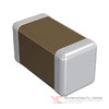
Product Overview – Murata GQM1555C2A390GB01D
Murata GQM1555C2A390GB01D is a High Q and High Power Chip Multilayer Ceramic Capacitor designed for general electronic equipment, with a particular fit for RF and high-frequency applications.
Key device parameters for GQM1555C2A390GB01D:
- Capacitance: 39 pF
- Tolerance: ±2 %
- Rated voltage: DC 100 V
- Dielectric: C0G/NP0 (EIA C0G)
- Package size: 0402 (1005 metric, Murata GQM15 size code)
The C0G/NP0 dielectric provides minimal capacitance variation with temperature, low dielectric loss, and stable behavior over time and applied voltage. Combined with the High Q / High Power design concept of the GQM series, GQM1555C2A390GB01D is suited to resonance circuits, impedance matching networks, and other frequency-sensitive nodes where loss and stability must be tightly controlled.
Murata positions GQM1555C2A390GB01D within its High Q and High Power GQM series for general-purpose usage, with the documentation explicitly advising users to confirm specifications and approval sheets as of the stated issue date, since product data can change without notice.
---
2.
Construction and Dimensional Profile of GQM1555C2A390GB01D
GQM1555C2A390GB01D is a chip multilayer ceramic capacitor in 0402 (1005 metric) format, denoted in the Murata internal type system as GQM15. Although the datasheet excerpt references “Type & Dimensions” rather than listing numbers, GQM1555C2A390GB01D follows standard 0402 geometry:
- Length and width: conforming to 1.0 mm × 0.5 mm class
- Terminations: external electrodes suitable for Sn-3.0Ag-0.5Cu lead-free solder
- Multilayer structure: stacked internal electrodes and C0G ceramic layers optimized for High Q / High Power behavior
The small footprint of GQM1555C2A390GB01D allows placement close to RF active devices and in dense high-speed layouts. At the same time, the mechanical sensitivity associated with direct surface mounting (as opposed to leaded devices) makes PCB design, land pattern selection, and solder amount particularly relevant for long-term reliability.
Murata’s cautions around board bending, thermal shock, and solder fillet height for GQM1555C2A390GB01D are direct consequences of this compact multilayer construction and the nature of ceramic dielectric materials.
---
3.
Electrical Ratings and Temperature Characteristics of GQM1555C2A390GB01D
GQM1555C2A390GB01D is defined as:
- 39 pF nominal capacitance
- ±2 % capacitance tolerance
- Rated DC voltage: 100 V
- Dielectric: C0G/NP0
Operating temperature for GQM1555C2A390GB01D is governed by Murata’s “Rating – Operating Temperature” guidance:
- Do not exceed the maximum operating temperature assigned to the specific capacitor type.
- The capacitor surface temperature, including self-heating, must remain within the specified operating limit.
For C0G/NP0, temperature-dependent capacitance variation is inherently small, and the documentation emphasizes issues for “high dielectric constant type capacitors”. Although GQM1555C2A390GB01D uses C0G (which is not a high-K class), the same framework applies:
- Capacitance changes with temperature should be considered, and suitable capacitance chosen for the actual operating temperature range.
- Selection for time-constant or resonance circuits should always be confirmed under real operating temperature distribution in the equipment.
Murata recommends measuring capacitance of GQM1555C2A390GB01D under specified test conditions (voltage and frequency) and verifying that the measurement equipment delivers the prescribed test voltage, especially when capacitance values are high. For C0G 39 pF, measurement loading is usually non-problematic, but system-level verification remains advised.
Since C0G/NP0 has negligible aging, the detailed “Capacitance Aging” discussion primarily targets high dielectric constant types; GQM1555C2A390GB01D does not exhibit significant time-dependent drop in capacitance under normal conditions, which is advantageous for RF filters and oscillators that must sustain tuning over product lifetime.
---
4. Voltage, Current, and Self-Heating Behavior of GQM1555C2A390GB01D
GQM1555C2A390GB01D must be operated within its 100 V DC rating with the following applied-voltage rules:
- DC plus superimposed AC: the zero-to-peak value must not exceed 100 V DC.
- Pure AC or pulse: the peak-to-peak voltage must not exceed 100 V DC.
- Abnormal voltages (surge, ESD, pulse spikes) must also be kept within the rated voltage.
Murata notes that overvoltage on capacitors like GQM1555C2A390GB01D can lead to dielectric breakdown and short circuits, with time-to-failure decreasing as both applied voltage and ambient temperature increase.
When GQM1555C2A390GB01D is used in AC or pulse circuits, the capacitor experiences ripple current and may self-heat due to dielectric and ESR-related losses. Murata specifies that:
- Self-heating temperature rise of the capacitor body, measured at 25 °C ambient, should be kept below 20 °C.
- The total surface temperature of GQM1555C2A390GB01D, including ambient and self-heating, must remain below its maximum operating temperature.
For example, in a high-frequency matching network with several volts of RF across GQM1555C2A390GB01D, designers should measure its surface temperature under worst-case drive conditions and adjust circuit Q or component placement if the rise approaches 20 °C.
The documentation describes substantial DC and AC voltage dependence and aging for high dielectric constant types. For C0G-based GQM1555C2A390GB01D, voltage and aging effects are much smaller, making it suitable for high-stability RF nodes where capacitance drift due to voltage swing would otherwise detune circuits.
---
5. Reliability, Mechanical Stress, and Board-Level Behavior of GQM1555C2A390GB01D
The datasheet devotes extensive content to mechanical stress and its link to electrical failures for chip MLCCs like GQM1555C2A390GB01D. Key reliability factors:
- Substrate bending:
- Substrate bending tests are described using FR-4 glass epoxy boards (0.8 mm or 1.6 mm thick) with standard copper thickness (0.035 mm).
- Stress from board flexing can induce internal cracks in GQM1555C2A390GB01D, leading to reduced insulation resistance or shorts.
- Shock and vibration:
- Vibration, substrate bending, and shock are considered in qualification tests (adhesive strength of termination, vibration, temperature sudden change, high temperature/high humidity, durability).
- Boards that are bent or twisted during cropping, handling, test probing, or screw tightening can damage GQM1555C2A390GB01D.
- Board handling and stacking:
- When stacked PCBs contact each other, the corner of one board should not hit the capacitor on another.
- Dropped boards or capacitors must not be reused, since damage may be latent and degrade long-term reliability.
Real-world example: a small RF module with GQM1555C2A390GB01D placed near a V-groove separation line can develop cracks during panel depanelization if a simple hand-bending separation method is used. Transitioning to a router-type separator, or reorienting the component parallel to the separation line with additional slits, can significantly reduce the strain experienced by the capacitor.
Testing and production processes for GQM1555C2A390GB01D must therefore be designed to minimize PCB strain and local mechanical impacts, from pick-and-place through final assembly and field operation.
---
6.
Soldering, Reflow, and Flow Processes for GQM1555C2A390GB01D
GQM1555C2A390GB01D is compatible with lead-free soldering processes, particularly Sn-3.0Ag-0.5Cu. The datasheet describes:
Reflow soldering for GQM1555C2A390GB01D:
- Preheating is required to minimize thermal shock; both PCB and component temperatures should be controlled to keep the temperature differential (ΔT) between solder and component surface as small as possible.
- Recommended reflow profiles specify allowable peak temperature and time; repeated reflow is permitted provided total soldering time remains within specified limits.
- If peak temperature on GQM1555C2A390GB01D is lower than the solder manufacturer’s specified peak, several issues can appear:
- Reduced solder wettability
- Solder voids and reduced bonding strength
- Whisker risk
- Reduced self-alignment, leading to tombstoning or component shift
Solder amount for GQM1555C2A390GB01D in reflow:
- Excess solder thickness increases solder fillet height and stresses the chip during board bending or thermal expansion, raising crack risk.
- Insufficient solder weakens mechanical anchoring, enabling detachment or poor electrical contact.
- Solder height should remain below the thickness of the capacitor, with a smooth fillet reaching the end surface of the chip.
Flow soldering and GQM1555C2A390GB01D:
- Flow soldering methods are generally limited to chip sizes from 1.6 × 0.8 mm to 2.0 × 1.25 mm, based on the land design tables. GQM1555C2A390GB01D is 0402 and significantly smaller, so reflow is typically the appropriate process.
- Where flow soldering is applicable for other GQM sizes, Murata specifies preheating, solder temperature/time, and leaching limits to protect terminations. These principles apply philosophically to GQM1555C2A390GB01D: minimize thermal shock and keep termination leaching under control.
Rework of GQM1555C2A390GB01D:
- Rework soldering requires preheating and controlled soldering iron conditions:
- Preheat to a specified range (Table 3 in the datasheet) to limit ΔT between soldering tip and component.
- Use a soldering iron with a tip diameter ≤ 3 mm and solder wire ≤ 0.5 mm.
- Avoid direct contact between iron tip and the ceramic body.
- Spot heater (hot air) rework:
- Reduces local thermal shock by heating component and board more uniformly.
- Distance, temperature, and air direction (as illustrated in Table 4 and Figure 1) are set to control ΔT and solder fillet shape.
In production, a typical sequence for GQM1555C2A390GB01D would use stencil-printed lead-free paste, controlled reflow according to Murata’s recommended profile, and no flow soldering on this 0402 size.
---
7.
PCB Design, Land Pattern, and Adhesive Use with GQM1555C2A390GB01D
PCB design for GQM1555C2A390GB01D focuses on strain management and land geometry.
Land pattern considerations for GQM1555C2A390GB01D:
- Chip components like GQM1555C2A390GB01D are directly mounted and therefore susceptible to flexing stress from the PCB.
- Excess solder fillet height, determined by land pattern and paste aperture, can amplify these stresses.
- Murata provides land design tables for flow and reflow methods; for 0402-class GQM1555C2A390GB01D, reflow land recommendations should be followed and validated on the actual PCB.
- PCB bending resistance can be improved by using solder resist design to adjust certain land dimensions (e.g., “a” dimension in Table 1).
Mounting position for GQM1555C2A390GB01D:
- Orientation:
- Place GQM1555C2A390GB01D such that its long axis is parallel to the direction of board flexing stress during depanelization or handling, reducing stress concentration.
- Proximity to board separation lines:
- If GQM1555C2A390GB01D must be close to a V-groove or perforation, consider:
- Parallel orientation to separation direction
- Additional slits near the separation point
- Maximizing distance from the separation edge when possible
Adhesive use before soldering with GQM1555C2A390GB01D:
- For flow soldering or specific processes, temporary adhesive attachment may be considered. Though GQM1555C2A390GB01D is mainly reflow-soldered, the same adhesive rules apply:
- Epoxy resins are typical; selection criteria include:
1) Sufficient adhesive strength through mounting and soldering
2) Stability under moisture during soldering
3) Good coatability and shape retention
4) Long pot life and short curing time
5) Non-corrosive to capacitor and board, and with good insulation
6) No halogenated compounds and no toxic gas generation
- Excess adhesive that overflows onto the land can impair soldering and electrical contact.
- Inadequate adhesive (too little, insufficient area, under-cured) leads to device loosening or detachment.
- Overly high curing temperature or long curing time can oxidize terminations and board pads, harming solderability.
Board design factors such as PCB thickness, length and width directly affect total strain. Larger, thinner PCBs flex more, so high-density layouts including GQM1555C2A390GB01D should be evaluated with representative panel handling and depanelization methods.
---
8.
Cleaning, Coating, and Environmental Conditions for GQM1555C2A390GB01D
Cleaning GQM1555C2A390GB01D after soldering:
- Excessive ultrasonic cleaning can induce PCB resonance and cause cracks in GQM1555C2A390GB01D or break solder joints.
- Murata recommends:
- Evaluating the actual cleaning equipment and cycle with GQM1555C2A390GB01D-mounted boards.
- Ensuring that cleaning solvents do not leave flux residues or other contaminants that could degrade electrical performance or reliability.
- Avoiding improper (overly strong or insufficient) cleaning that can alter capacitor characteristics or leave harmful residues.
Flux and solder paste for GQM1555C2A390GB01D:
- Use flux sparingly and evenly; excessive flux promotes large gas evolution and poor solderability.
- Use flux with halide content ≤ 0.1 %.
- Do not use strong acidic or water-soluble (non-rosin-type) flux, for both flow and reflow soldering.
- Termination leaching must be limited to ≤ 25 % of the chip end area (as a single chip) and ≤ 25 % of the exposed edge length when mounted.
Coating over GQM1555C2A390GB01D:
- Resins used for coating or molding can induce stress during curing due to thermal contraction, which may crack or delaminate GQM1555C2A390GB01D or lower insulation resistance.
- Recommended resin properties:
- Low curing contraction
- Thermal expansion coefficient close to that of the capacitor
- Low hygroscopicity
- Non-strong-acid, low-halogen systems
- Silicone resin can serve as an under-coating layer to buffer stress from the main coating.
- Epoxy resins with low hygroscopicity can reduce insulation resistance degradation in humid environments.
Environmental and storage conditions for GQM1555C2A390GB01D:
- Storage:
- Temperature: +5 °C to +40 °C
- Relative Humidity: 20 % to 70 %
- Keep in original packaging; avoid direct sunlight, high humidity, and corrosive atmospheres (H₂S, SO₂, Cl₂, NH₃, etc.).
- Long storage can oxidize terminations and degrade taping; if > 6 months from delivery, check mounting; if > 1 year, also confirm solderability.
- Operation atmosphere:
- Avoid environments with water or oil splashes, direct sunlight, ozone, UV, radiation, toxic gases, condensation, excessive vibration or shock.
- Use damp-proof measures if condensation is possible.
These constraints ensure GQM1555C2A390GB01D retains its high insulation resistance and stable capacitance over lifetime.
---
9.
Packaging, Taping, and Handling of GQM1555C2A390GB01D
GQM1555C2A390GB01D uses tape carrier packaging appropriate for 0402 devices within the GQM type:
- Tape carrier packaging codes: D, E, W, L, J, F, K (with W specified as paper tape W8P1 for GQM15).
- Typical characteristics:
- Minimum quantity per reel defined per GQM type (GQM15 for GQM1555C2A390GB01D).
- Paper or plastic tape with specified cavity dimensions for 0402 size.
- Tapes wound clockwise, sprocket holes on the right when tape is pulled toward the operator.
- Leader and vacant sections at the start of the reel, with defined lengths for automatic feeder setup.
- Accumulated pitch of 10 sprocket holes = 40 ± 0.3 mm.
- Chips enclosed by top and bottom tape; no jointing in top or bottom tape; cavities are free from fuzz.
- Breakdown force of top tape: ≥ 5 N; bottom tape: ≥ 5 N where present.
- Peel-off force of top tape: 0.1 N to 0.6 N in the specified direction.
- Reels made of resin; dimensions defined in Murata’s reel drawing, with possible material/dimension changes.
Labeling for GQM1555C2A390GB01D reels includes customer part number, Murata part number, company name, inspection number, and quantity.
In practice, automated pick-and-place of GQM1555C2A390GB01D relies on these tape features to maintain accurate feed, minimize chip damage, and support high-speed assembly.
---
10.
Application Boundaries and Circuit Design Considerations for GQM1555C2A390GB01D
Limitations of applications for GQM1555C2A390GB01D:
Murata requests prior consultation before using products like GQM1555C2A390GB01D in equipment requiring especially high reliability where failure could directly cause harm to life, body, or property. The listed categories include:
1) Aircraft equipment
2) Aerospace equipment
3) Undersea equipment
4) Power plant control equipment
5) Medical equipment
6) Transportation equipment (vehicles, trains, ships)
7) Traffic signal equipment
8) Disaster prevention / crime prevention equipment
9) Data-processing equipment
10) Other applications with comparable reliability demands
Circuit design guidelines for GQM1555C2A390GB01D:
- Fail-safe functions:
- Cracks from dropping or PCB bending can reduce insulation resistance and lead to shorts.
- In circuits where such a short could cause electric shock, smoke, or fire, additional fail-safe measures such as fuses should be implemented.
- GQM1555C2A390GB01D and its series are not safety standard certified; external safety design must cover worst-case failure modes.
- Applied voltage and surge:
- Ensure surge voltages generated by inductances in the system do not exceed the 100 V DC rating of GQM1555C2A390GB01D.
- Evaluate surge resistance in the actual system as required.
- Piezo-electric phenomenon:
- High dielectric constant capacitors can generate audible noise or vibration when used in AC or pulse circuits, and when mechanical shock is applied.
- GQM1555C2A390GB01D uses C0G, which has lower piezoelectric effects than high-K types; nonetheless, in high-frequency or mechanically severe environments, system evaluation is recommended.
An example is a DC-DC converter or RF power stage where GQM1555C2A390GB01D is used at nodes with high dv/dt. Surge transient analysis must confirm that the capacitor is not overstressed by switching transients or ESD events.
---
11. System-Level Evaluation and Long-Term Performance of GQM1555C2A390GB01D
Murata strongly advises system-level evaluation for GQM1555C2A390GB01D:
- Evaluate capacitance, leakage current, and noise absorption under actual voltage, temperature, and frequency conditions present in the final product.
- Consider that capacitance of high dielectric devices varies with voltage and temperature; while GQM1555C2A390GB01D is C0G and stable, nearby components may not be, and system performance can depend on the entire network.
- Confirm that surge events, including those caused by wiring inductance or switching, stay within the capacitor’s rated voltage and thermal limits.
Transportation and handling of assemblies with GQM1555C2A390GB01D:
- During shipment and logistics, maintain environmental conditions:
- Low air temperature down to -40 °C
- Temperature change of -25 °C/+25 °C
- Air pressure as low as 30 kPa
- Pressure change up to 6 kPa/min
- Packaging must prevent deformation that transfers mechanical forces onto the capacitors.
- Avoid excessive vibration, shock, or pressure, as sharp impacts from tools or chassis edges can cause cracking and potential short circuits.
- Do not use capacitors that have experienced unknown mechanical shock (e.g., dropped reels or boards).
Under operation of equipment containing GQM1555C2A390GB01D:
- Do not touch capacitors directly during operation (shock hazard).
- Avoid exposure to conductive or corrosive liquids.
- Apply damp-proof measures for environments where condensation can occur.
Overall system reliability with GQM1555C2A390GB01D depends on adherence to these handling, environmental, and evaluation practices.
---
12.
Conclusion – Effective Use of GQM1555C2A390GB01D in RF and General Electronics
GQM1555C2A390GB01D combines a 39 pF ±2 % C0G/NP0 dielectric with High Q and High Power design in a compact 0402 (GQM15) chip format and a 100 V DC rating. This profile supports its use in RF filters, impedance matching networks, high-frequency resonators, and other circuits that require low-loss, stable capacitance with fine tolerance.
The Murata documentation surrounding GQM1555C2A390GB01D emphasizes that electrical stability must be matched by mechanically and thermally robust implementation. PCB design, solder amount, handling, cleaning, coating, and environmental control are all tightly interlinked with long-term reliability and must be managed within the provided guidelines.
When these design and process conditions are respected, GQM1555C2A390GB01D can be deployed effectively in general electronic equipment, particularly where high-frequency performance and stability are central to system behavior.
---
Frequently Asked Questions (FAQ)
- Q1. What are the basic electrical specifications of GQM1555C2A390GB01D?
-
- A1. GQM1555C2A390GB01D is a High Q and High Power chip multilayer ceramic capacitor with a nominal capacitance of 39 pF, capacitance tolerance of ±2 %, rated DC voltage of 100 V, and C0G/NP0 dielectric. It is packaged in a 0402 (1005 metric, GQM15) surface-mount case.
- Q2. In what kind of circuits is GQM1555C2A390GB01D typically used?
-
- A2. GQM1555C2A390GB01D belongs to Murata’s High Q and High Power GQM series for general electronic equipment. Its 39 pF C0G/NP0 profile and high-voltage capability make it suitable for RF matching networks, filters, oscillators, resonance circuits, and other high-frequency nodes that benefit from low loss and tight capacitance tolerance.
- Q3. How stable is the capacitance of GQM1555C2A390GB01D over temperature?
-
- A3. GQM1555C2A390GB01D uses C0G/NP0 dielectric, which exhibits minimal temperature dependency compared to high dielectric constant types. The datasheet’s temperature-dependence warnings are primarily aimed at high-K capacitors; for GQM1555C2A390GB01D, temperature-induced variation is small, and there is no significant capacitance aging, making it well suited to precision and RF applications.
- Q4. Can GQM1555C2A390GB01D be used in circuits with large AC or RF voltages?
-
- A4. Yes, provided the applied voltage (including DC plus AC peaks or pulse peaks) does not exceed the 100 V DC rating. In AC or RF applications, GQM1555C2A390GB01D carries ripple current and can self-heat. Murata specifies that the self-heating temperature rise should be limited to less than 20 °C at 25 °C ambient and that total surface temperature must remain within the operating limit. Surface temperature should be measured under worst-case conditions in the actual circuit.
- Q5. How should GQM1555C2A390GB01D be mounted to minimize cracking due to PCB bending?
-
- A5. To reduce mechanical stress on GQM1555C2A390GB01D, orientation and position should be carefully chosen:
- Mount the capacitor so that its long axis is parallel to the main direction of PCB flexing.
- Avoid placing GQM1555C2A390GB01D close to V-grooves or perforated separation lines; if unavoidable, use slits and parallel mounting near separation edges.
- Keep GQM1555C2A390GB01D away from screw holes and areas that experience board bending when screws are tightened.
- Use router-type separators or well-designed jigs for depanelization to limit stress. - Q6. What soldering processes are recommended for GQM1555C2A390GB01D?
-
- A6. GQM1555C2A390GB01D (0402) is best mounted using lead-free reflow soldering with Sn-3.0Ag-0.5Cu solder. Preheating is required to avoid thermal shock, and reflow profile must meet Murata’s recommended peak temperature and time limits. Flow soldering is generally recommended only for larger chip sizes (1.6 × 0.8 mm to 2.0 × 1.25 mm), so it is not the primary method for this 0402 capacitor.
- Q7. How much solder should be used with GQM1555C2A390GB01D?
-
- A7. Solder volume for GQM1555C2A390GB01D should be controlled so that:
- The solder fillet height remains below the thickness of the capacitor.
- The fillet is smooth and reaches the end surface of the chip without excessive rise.
Excess solder increases stress during board bending and temperature cycling, raising crack risk. Insufficient solder can lead to weak bonding and possible detachment or poor contact. - Q8. Is rework of GQM1555C2A390GB01D with a soldering iron allowed?
-
- A8. Yes, rework is allowed with precautions:
- Preheat GQM1555C2A390GB01D and the PCB to the specified range to limit thermal gradients.
- Use a soldering iron tip ≤ 3 mm diameter and solder wire ≤ 0.5 mm.
- Avoid direct contact between the iron tip and the capacitor body.
- Keep soldering time as short as possible to prevent termination leaching and strength degradation.
Hot air spot heaters can also be used to reduce thermal shock if conditions in the datasheet are followed. - Q9. What flux types are suitable for soldering GQM1555C2A390GB01D?
-
- A9. For GQM1555C2A390GB01D, use flux with halide content ≤ 0.1 %, applied thinly and evenly. Do not use strong acidic flux or water-soluble (non-rosin-type) flux for either flow or reflow, as these can corrode terminations or leave harmful residues. Flux and solder paste compositions should be evaluated with the actual process.
- Q10. How should GQM1555C2A390GB01D be cleaned after soldering?
-
- A10. Cleaning processes for GQM1555C2A390GB01D must be validated on actual boards. Excessive ultrasonic power can cause PCB resonance and crack the capacitor or break solder joints. The chosen solvent should effectively remove flux without leaving residues or attacking terminations or coatings. Cleaning time and conditions must avoid both under-cleaning and over-cleaning, which can affect capacitor performance.
- Q11. Can GQM1555C2A390GB01D be coated or potted?
-
- A11. Yes, but resin selection is important:
- Use resins with low curing contraction and thermal expansion coefficients close to that of the capacitor.
- Prefer low-hygroscopic materials (e.g., suitable epoxy resins) to maintain insulation resistance in humid conditions.
- Avoid strong acidic and high-halogen coatings.
- Silicone resins can be used as under-coating to buffer stress.
Improper coating can crack GQM1555C2A390GB01D or cause peeling and insulation deterioration. - Q12. What storage conditions are recommended for GQM1555C2A390GB01D?
-
- A12. GQM1555C2A390GB01D should be stored in original packaging at +5 °C to +40 °C and 20 % to 70 % relative humidity, away from direct sunlight, high humidity, and corrosive gases such as hydrogen sulfide, sulfur dioxide, chlorine, or ammonia. Long storage can oxidize terminations and degrade taping. If more than six months have passed since delivery, mounting should be checked; if more than one year, solderability should also be confirmed.
- Q13. Are there application categories where GQM1555C2A390GB01D should not be used without consultation?
-
- A13. Yes. Murata requests consultation before using GQM1555C2A390GB01D in applications that require especially high reliability to prevent failures that could directly affect human life or major property. These include aircraft, aerospace, undersea systems, power plant control, medical equipment, transport equipment, traffic signals, disaster/crime prevention, data-processing equipment, and applications of similar complexity and reliability requirement.
- Q14. Does GQM1555C2A390GB01D require external protection in safety-related circuits?
-
- A14. Because GQM1555C2A390GB01D and its series are not safety standard certified and may fail short when cracked or overstressed, circuits that could cause electric shock, smoke, or fire during a capacitor short should include fail-safe features, such as fuses or protective elements. System-level safety design should assume potential short failures of the capacitor.
- Q15. How should GQM1555C2A390GB01D be evaluated in the final system?
-
- A15. Before volume production, GQM1555C2A390GB01D should be evaluated in the final system under actual electrical, thermal, and mechanical conditions. This includes verifying capacitance stability, leakage current, noise absorption, behavior under expected surges, thermal cycling, board flexing, and any cleaning or coating steps. Such evaluation ensures that the capacitor operates within the limits defined in its product specification throughout the product’s service life.