Infineon Technologies CY7C53150 and CY7C53120 product overview
2.
Infineon Technologies CY7C53150 and CY7C53120 functional role in LonWorks distributed control networks
The CY7C53150 and CY7C53120 are intended to form the processing and networking core of LonWorks nodes. Their design combines node control, communications handling, and protocol execution into a single device, reducing the amount of external logic required in distributed control applications.
A central part of this role is the LonTalk protocol firmware. Services at every layer of the OSI networking reference model are implemented in this firmware. In the CY7C53120E2 and CY7C53120E4, the LonTalk firmware is stored in on-chip ROM, with 10 KB ROM in the CY7C53120E2 and 12 KB ROM in the CY7C53120E4. In the CY7C53150, the firmware resides in off-chip memory.
The firmware also includes 34 preprogrammed I/O drivers. This reduces application-level software overhead because many interface behaviors are already available in the device firmware. Application programs are stored in Flash memory in the CY7C53120 family and in Flash plus off-chip memory for the CY7C53150. The documentation also states that application code may be updated by downloading over the network, which supports systems where field updates are part of the deployment model.
In practical terms, this means a LonWorks node can be designed with the CY7C531x0 handling both network protocol tasks and local control behavior. For example, a node connected to building control wiring or industrial sensing equipment can process local I/O events while simultaneously handling LonTalk network messaging without requiring a separate communications controller.
Infineon Technologies CY7C53150 and CY7C53120 processing architecture and integrated resources
The CY7C531x0 family uses three 8-bit pipelined processors. This architecture is described as supporting concurrent processing of application code and network traffic. Rather than time-sharing all workloads through a single small controller, the device allocates processing capability in a way that better matches communication-heavy distributed node behavior.
The integrated resource set includes:
2,048 bytes of SRAM for buffering network data, system data, and application data storage
Two 16-bit timer/counters for measuring and generating I/O device waveforms
An 11-pin I/O port programmable in 34 modes
A 5-pin communication port for direct connection to network transceiver interfaces
A unique 48-bit ID number in every device to support network installation and management
The SRAM serves several roles at once, including network data buffering and storage of system and application data. This arrangement fits node-level control products where transient communications and local state information must coexist in a limited memory footprint.
The timer/counter resources allow waveform generation and measurement. The output of Timer/Counter 1 may be routed to I/O0, and the output of Timer/Counter 2 may be routed to I/O1. Input sources for the timer/counters can also be derived from selected I/O pins. This gives the device a path to interact with pulse-based signals, timing events, or externally driven waveform activity.
The 48-bit unique ID helps with network installation and management. In distributed networks with many nodes, a built-in unique identifier provides a hardware-level identity anchor that the network can use for device distinction and configuration workflows.
Infineon Technologies CY7C53150 and CY7C53120 memory organization, firmware placement, and application storage
Memory organization is one of the main distinctions between the CY7C53150 and CY7C53120 variants.
For all Neuron chips, system firmware must be available at power-up. In the CY7C53120 family, this firmware is factory-programmed in on-chip ROM. In the CY7C53150, the system firmware must be stored in the first 16 KB of off-chip nonvolatile memory such as Flash, EPROM, EEPROM, or NVRAM. These memory devices must be programmed in a device programmer before board assembly. Because the system firmware implements the network protocol, it cannot be downloaded over the network.
For user applications, the CY7C53120 family stores application code in on-chip Flash memory. This code may be programmed before assembly using a device programmer or downloaded and updated over the LonTalk network from an external network management tool.
For the CY7C53150, the user application program is stored in on-chip Flash memory and also in off-chip memory. The off-chip memory can be initially programmed using a device programmer.
The family-level memory capacities described in the documentation include:
512 bytes of Flash memory for the CY7C53150
2,048 bytes of Flash memory for the CY7C53120E2
4,096 bytes of Flash memory for the CY7C53120E4
10 KB of ROM containing LonTalk firmware for the CY7C53120E2
12 KB of ROM containing LonTalk firmware for the CY7C53120E4
A useful way to read this partitioning is to separate network protocol storage from application storage. In the CY7C53120 devices, protocol firmware is fixed on chip, while user application space is provided in Flash. In the CY7C53150, larger programs can be supported by placing system firmware and expanded application content in external memory.
Infineon Technologies CY7C53150 and CY7C53120 communications port modes and transceiver interfacing
The 5-pin communications port is one of the defining interface blocks in the CY7C531x0 family. It is designed to connect to a variety of network media transceivers and supports three operating modes.
The documentation lists common transceiver media as twisted-pair, powerline, RF, IR, fiber-optics, and coaxial. This gives the family flexibility across multiple physical network implementations.
In Single-Ended Mode:
CP0 is used for receiving serial data
CP1 is used for transmitting serial data
CP2 enables an external transceiver
Data uses Differential Manchester encoding
In Special Purpose Mode:
CP0 receives serial data
CP1 transmits serial data
CP2 transmits a bit clock
CP4 transmits a frame clock for use by an external intelligent transceiver
The external transceiver is responsible for encoding and decoding the data stream
In Differential Mode:
CP0 and CP1 form a differential receiver
The receiver includes built-in programmable hysteresis and low-pass filtering
CP2 and CP3 form a differential driver
Serial data uses Differential Manchester encoding
The Differential Mode includes programmable receiver behavior. The datasheet provides hysteresis values expressed as differential peak-to-peak voltages in terms of VDD, as well as programmable glitch filter values expressed as transient pulse suppression times. For example, the receiver hysteresis settings range upward through several selectable levels, and glitch filtering ranges from a typical 75 ns at filter setting 0 to a typical 1500 ns at filter setting 3. The documentation notes that the glitch filter must be disabled if the data rate is 1.25 Mbps or greater.
This configurability allows the communications interface to be tuned to line characteristics and noise conditions. As an example, a noisier cabling environment may benefit from increased hysteresis or filtering, while a higher-speed link may require reduced filtering to preserve signal integrity and timing.
Infineon Technologies CY7C53150 and CY7C53120 I/O structure, timers, and application interfacing flexibility
The CY7C531x0 family provides a set of general-purpose and function-sharing I/O pins intended to support application interfacing with a relatively small external component count.
The I/O structure includes:
I/O0 to I/O3, which provide large current-sink capacity of 20 mA
I/O4 to I/O7, which include built-in programmable pull-ups
I/O8 to I/O10, which may be used for serial communication under firmware control
The documentation describes the 11-pin I/O port as programmable in 34 modes. This broadens the range of direct sensor, actuator, and logic interfacing options available to the device.
Timer/counter integration further extends the I/O behavior:
The output of Timer/Counter 1 may be routed to I/O0
The output of Timer/Counter 2 may be routed to I/O1
The input to Timer/Counter 1 may be derived from one of I/O4 to I/O7
The input to Timer/Counter 2 may be derived from I/O4
This arrangement supports designs where some pins must alternate between ordinary digital I/O and timing-related roles. For instance, a node may use one pin to generate a periodic waveform while another measures incoming pulse activity, all without an additional timing IC.
The RESET pin is an active-low I/O pin with a built-in pull-up. The allowable external capacitance connected to RESET is 100 pF to 1000 pF. The SERVICE pin is also active low, has a built-in configurable pull-up, and alternates between input and output at a 76 Hz rate.
Infineon Technologies CY7C53150 and CY7C53120 external memory capability and replacement compatibility
The CY7C53150 differs from the CY7C53120 family by incorporating an external memory interface. This allows the device to address up to 64 KB of external memory, with 6 KB of the address space mapped internally. A feature summary line also states that the CY7C53150 addresses up to 58 KB of external memory, reflecting the effect of internal mapping within the total addressable space.
This external memory capability is intended for LonWorks nodes that require larger application programs. In such systems, the device can combine its on-chip resources with off-chip storage for firmware and user code.
The CY7C53150 exposes a bidirectional memory data bus D0 to D7, read/write control output R/W, output enable clock control E, and memory address outputs A0 to A15. These signals are available in the 64-pin TQFP package and form the basis of the external memory subsystem.
The documentation also specifies compatibility relationships:
The CY7C53150 Neuron chip is an exact replacement for the Motorola MC143150Bx and Toshiba TMPN3150B1 devices
The CY7C53120E2 Neuron chip is an exact replacement for the Motorola MC143120E2 device because it contains the same firmware in ROM
For legacy designs, this replacement compatibility can simplify migration. A design already using one of the listed earlier devices can potentially move to the Infineon Technologies part while preserving system-level architecture and expected firmware behavior, subject to the documented device characteristics and package details.
Infineon Technologies CY7C53150 and CY7C53120 Flash retention, endurance, and write behavior
The Flash memory behavior described in the documentation provides a clearer picture of how the devices handle code and data updates over time.
Data and code stored in Flash memory are guaranteed to be retained for at least 10 years for a programming temperature range of –25°C to 85°C. The Flash memory can typically be written 100,000 times without data loss. An erase/write cycle takes 20 ms.
The documentation also explains two firmware-level mechanisms that extend effective Flash endurance.
First, if the data being written to a Flash byte is the same as the data already present, the firmware does not perform the physical write. This means repeated attempts to store unchanged values do not consume write cycles. A practical example given is an application that sets its own address in Flash memory after every reset: if the address has not changed, no write cycle is used.
Second, for CY7C53120E4 devices running system firmware version 13.1 or higher, writes to eight successive address locations can be aggregated into a single write. The documentation gives the example that downloading 4 KB of code over the network would result in only 512 writes rather than 4,096.
These details matter when evaluating update frequency and expected nonvolatile memory wear. The raw endurance number gives one baseline, but actual service life can be longer when applications frequently rewrite unchanged data or when the firmware’s aggregation behavior reduces the number of physical write operations.
Infineon Technologies CY7C53150 and CY7C53120 clocking, 40 MHz operation, and reset behavior
Clocking is handled through CLK1 and CLK2. CLK1 is the oscillator connection or external clock input, and CLK2 is the oscillator connection output. When an external clock is applied to CLK1, CLK2 should be left open, with a maximum of one external load.
The product family supports different maximum input clock frequencies:
20 MHz for the CY7C53150
10 MHz for the CY7C53120E2
40 MHz for the CY7C53120E4
The documentation includes a specific note for 40 MHz CY7C53120E4-40 operation. This device was designed to run at frequencies up to 40 MHz using an external clock oscillator. External oscillators may take on the order of 5 ms to stabilize after power-up. The Neuron chip must be held in reset until the CLK1 input is stable. In some cases, this may require a reset-stretching low-voltage detection chip or circuit. The oscillator vendor’s startup stabilization specification should be checked.
This startup behavior is a practical integration detail. If reset is released before the clock has stabilized, the device may begin operation under uncertain timing conditions. In a design using an external oscillator module, one straightforward interpretation is that reset timing should be based not only on supply rise time but also on oscillator stabilization time.
The documentation also notes a sleep-mode-related caution: rare combinations of wake-up events occurring during the go-to-sleep sequence could produce unexpected sleep behavior.
Infineon Technologies CY7C53150 and CY7C53120 low-voltage inhibit operation and operating conditions
The CY7C531x0 family includes an on-chip low-voltage inhibit or low-voltage detection function intended to protect nonvolatile memory behavior during supply disturbances.
The on-chip Low-voltage Inhibit circuit trips the Neuron chip whenever VDD is less than 4.1 V ± 0.3 V. According to the documentation, this prevents corruption of nonvolatile memory during voltage drops.
The devices operate from a 5.0 V nominal supply. The summary table shows the supply voltage as 4.5 V and above, and the operating temperature range is –40°C to 85°C. A note also specifies a maximum junction temperature of 105°C, with thermal calculations based on package thermal resistance:
32-pin SOIC: θJA = 51°C/W
44-pin TQFP: θJA = 43°C/W
64-pin TQFP: θJA = 44°C/W
This means ambient operating conditions and power dissipation should be considered together during thermal evaluation. The junction temperature relationship is given as TJunction = TAmbient + V · θJA as presented in the documentation note.
The family is described as having low operating current and supporting sleep mode operation for reduced current consumption.
Infineon Technologies CY7C53150 and CY7C53120 package options, pin functions, and implementation notes
Package selection depends on the device variant.
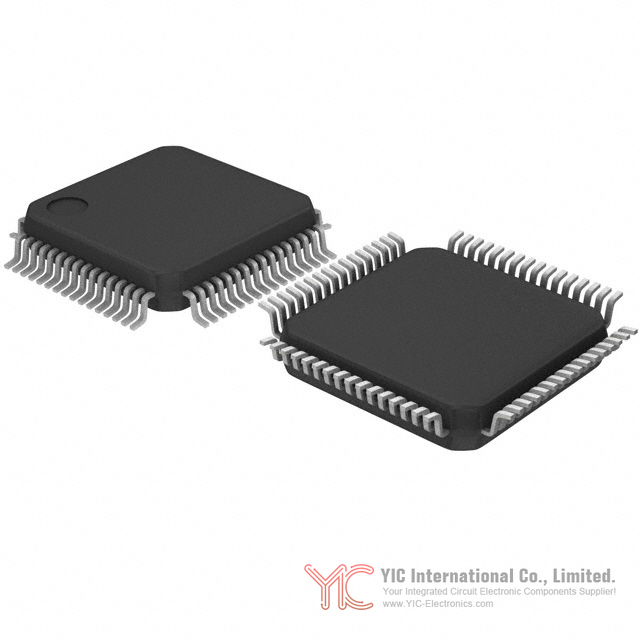
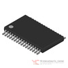
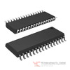
The CY7C53150 is offered in a 64-pin TQFP package. The CY7C53120 family is available in 32-pin SOIC or 44-pin TQFP packages. The package style information shown includes 64-LQFP / 64-TQFP (14x14) for the CY7C53150 and the SOIC/TQFP options for the CY7C53120.
Several pin-level implementation details from the documentation are worth capturing in one place:
All VDD pins must be connected together externally.
All VSS pins must be connected together externally.
NC pins must not be connected on the user’s PCB because they may be connected internally to the chip.
VPP is used for in-circuit test mode control. If VPP is high when RESET is asserted, the I/O, address, and data buses become high impedance.
The communication port uses CP0 to CP4.
The CY7C53150 provides external address and data bus pins that are not present on CY7C53120 variants.
For pin functions:
CLK1 is input for oscillator or external clock
CLK2 is oscillator output
RESET is active low with built-in pull-up
SERVICE is active low and alternates between input and output at 76 Hz
I/O0 to I/O3 support 20 mA sink current
I/O4 to I/O7 include configurable pull-ups
I/O8 to I/O10 can support serial communication under firmware control
These details influence schematic capture and PCB layout. For example, because NC pins must remain unconnected, treating them as spare tie points or routing anchors would conflict with the device guidance.
Conclusion
Infineon Technologies CY7C53150 and CY7C53120 integrate node control, communications handling, protocol execution, and application interfacing into a single Neuron Chip platform for LonWorks networks. The family combines three 8-bit pipelined processors, configurable communications support, programmable I/O, timer/counters, SRAM, nonvolatile memory resources, and a built-in unique identifier.
The main architectural split in the family is between the externally expandable CY7C53150 and the ROM-based CY7C53120 variants. The CY7C53150 is suited to designs that require off-chip firmware storage and larger external program space, while the CY7C53120E2 and CY7C53120E4 integrate LonTalk firmware in ROM and place user applications in on-chip Flash. Across the family, the communication port’s multiple operating modes, the programmable differential receiver characteristics, and the timer/I/O flexibility give designers multiple ways to match the device to different network media and local interface requirements.
At the implementation level, clock startup behavior, low-voltage inhibit protection, Flash endurance mechanisms, and package-specific pin functions define much of the practical integration work. Taken together, the documentation presents the CY7C53150 and CY7C53120 as specialized network processors designed to simplify the construction of LonWorks nodes while supporting a broad range of transceiver types and application configurations.
Frequently Asked Questions (FAQ)
- Q1. What is the primary difference between Infineon Technologies CY7C53150 and CY7C53120?
-
- A1. The main difference is memory architecture. The CY7C53120 family stores LonTalk protocol firmware in on-chip ROM and stores the user application in on-chip Flash memory. The CY7C53150 requires system firmware to be stored in the first 16 KB of off-chip nonvolatile memory and also supports external memory expansion for larger application programs.
- Q2. How many processors are integrated in the Infineon Technologies CY7C53150 and CY7C53120?
-
- A2. The CY7C531x0 family integrates three 8-bit pipelined processors. The documentation states that these are used for concurrent processing of application code and network traffic.
- Q3. How much SRAM is available in Infineon Technologies CY7C53150 and CY7C53120?
-
- A3. The family includes 2,048 bytes of SRAM. This SRAM is used for buffering network data and storing system and application data.
- Q4. What kinds of network media can Infineon Technologies CY7C53150 and CY7C53120 interface with?
-
- A4. The communication port can be configured to work with transceivers for twisted-pair, powerline, RF, IR, fiber-optics, and coaxial media.
- Q5. How does the communications port work in Single-Ended Mode on Infineon Technologies CY7C53150 and CY7C53120?
-
- A5. In Single-Ended Mode, CP0 receives serial data, CP1 transmits serial data, and CP2 enables an external transceiver. Data is communicated using Differential Manchester encoding.
- Q6. How does the communications port work in Special Purpose Mode on Infineon Technologies CY7C53150 and CY7C53120?
-
- A6. In Special Purpose Mode, CP0 receives serial data, CP1 transmits serial data, CP2 transmits a bit clock, and CP4 transmits a frame clock. In this mode, the external intelligent transceiver handles data encoding and decoding.
- Q7. How does the communications port work in Differential Mode on Infineon Technologies CY7C53150 and CY7C53120?
-
- A7. In Differential Mode, CP0 and CP1 form a differential receiver with programmable hysteresis and low-pass filtering, while CP2 and CP3 form a differential driver. Serial data uses Differential Manchester encoding.
- Q8. When should the programmable glitch filter be disabled on Infineon Technologies CY7C53150 and CY7C53120?
-
- A8. The documentation states that the glitch filter must be disabled if the data rate is 1.25 Mbps or greater.
- Q9. What is the maximum clock frequency for each Infineon Technologies CY7C531x0 variant?
-
- A9. The CY7C53150 supports up to 20 MHz, the CY7C53120E2 supports up to 10 MHz, and the CY7C53120E4 supports up to 40 MHz.
- Q10. What should be considered when using the Infineon Technologies CY7C53120E4 at 40 MHz?
-
- A10. The CY7C53120E4-40 is designed to run up to 40 MHz using an external clock oscillator. Because external oscillators may take around 5 ms to stabilize after power-up, the device must be held in reset until CLK1 is stable. Some oscillator choices may require a reset-stretching circuit.
- Q11. What is the low-voltage inhibit threshold for Infineon Technologies CY7C53150 and CY7C53120?
-
- A11. The on-chip Low-voltage Inhibit circuit trips when VDD is less than 4.1 V ± 0.3 V. This function is used to prevent nonvolatile memory corruption during voltage drops.
- Q12. How much Flash memory is available in each Infineon Technologies CY7C531x0 device?
-
- A12. The CY7C53150 includes 512 bytes of Flash memory, the CY7C53120E2 includes 2,048 bytes, and the CY7C53120E4 includes 4,096 bytes.
- Q13. How long is Flash data retention for Infineon Technologies CY7C53150 and CY7C53120?
-
- A13. Data and code stored in Flash memory are guaranteed to be retained for at least 10 years for a programming temperature range of –25°C to 85°C.
- Q14. What is the typical Flash endurance of Infineon Technologies CY7C53150 and CY7C53120?
-
- A14. The Flash memory can typically be written 100,000 times without data loss. The erase/write cycle time is 20 ms.
- Q15. How do Infineon Technologies CY7C53150 and CY7C53120 reduce unnecessary Flash wear?
-
- A15. The system firmware avoids a physical write if the new data is the same as the data already stored in a Flash byte. In addition, firmware version 13.1 or higher on CY7C53120E4 devices can aggregate writes to eight successive addresses into a single write.
- Q16. Can application code be updated over the network on Infineon Technologies CY7C53150 and CY7C53120?
-
- A16. Yes. For the CY7C53120 family, the user application stored in on-chip Flash may be downloaded and updated over the LonTalk network. The documentation also states that application code may be updated by downloading over the network. However, the system firmware that implements the network protocol cannot itself be downloaded over the network.
- Q17. What external memory types can be used with Infineon Technologies CY7C53150?
-
- A17. The CY7C53150 requires off-chip nonvolatile memory for system firmware, and the documentation lists Flash, EPROM, EEPROM, and NVRAM as suitable types.
- Q18. How much external memory can Infineon Technologies CY7C53150 address?
-
- A18. The documentation states that the CY7C53150 incorporates an external memory interface that can address up to 64 KB, with 6 KB of the address space mapped internally. A feature summary also states that it addresses up to 58 KB of external memory, reflecting the internal mapping within the overall address space.
- Q19. What package options are available for Infineon Technologies CY7C53150 and CY7C53120?
-
- A19. The CY7C53150 is available in a 64-pin TQFP package. The CY7C53120 is available in 32-pin SOIC or 44-pin TQFP packages.
- Q20. Which I/O pins on Infineon Technologies CY7C53150 and CY7C53120 provide higher sink current?
-
- A20. I/O0 through I/O3 provide large current-sink capacity of 20 mA.
- Q21. Which I/O pins on Infineon Technologies CY7C53150 and CY7C53120 have built-in pull-ups?
-
- A21. I/O4 through I/O7 have built-in configurable pull-ups.
- Q22. How are the timer/counters connected to I/O on Infineon Technologies CY7C53150 and CY7C53120?
-
- A22. Timer/Counter 1 output may be routed to I/O0, and Timer/Counter 2 output may be routed to I/O1. Timer/Counter 1 input may be derived from one of I/O4 through I/O7, and Timer/Counter 2 input may be derived from I/O4.
- Q23. What is the function of the SERVICE pin on Infineon Technologies CY7C53150 and CY7C53120?
-
- A23. SERVICE is an active-low pin with a built-in configurable pull-up. The documentation states that it alternates between input and output at a 76 Hz rate.
- Q24. What should be done with NC pins on Infineon Technologies CY7C53150 and CY7C53120?
-
- A24. NC pins must not be connected on the user’s PCB because they may be connected internally to the chip.
- Q25. What happens if VPP is high while RESET is asserted on Infineon Technologies CY7C53150 and CY7C53120?
-
- A25. If VPP is high when RESET is asserted, the I/O, address, and data buses become high impedance.
- Q26. Are Infineon Technologies CY7C53150 and CY7C53120 compatible with older devices?
-
- A26. Yes. The CY7C53150 is specified as an exact replacement for the Motorola MC143150Bx and Toshiba TMPN3150B1 devices. The CY7C53120E2 is specified as an exact replacement for the Motorola MC143120E2 because it contains the same firmware in ROM.
- Q27. What operating temperature range is specified for Infineon Technologies CY7C53150 and CY7C53120?
-
- A27. The specified operating temperature range is –40°C to 85°C. The documentation also notes a maximum junction temperature of 105°C.
- Q28. Do Infineon Technologies CY7C53150 and CY7C53120 support reduced-power operation?
-
- A28. Yes. The family is described as having low operating current and sleep mode operation for reduced current consumption. The documentation also notes that rare combinations of wake-up events occurring during the go-to-sleep sequence could produce unexpected sleep behavior.