Product Overview of the MC100LVEL51
The MC100LVEL51 is a differential clock D flip-flop with asynchronous reset, manufactured by onsemi as part of the 100 Series ECL logic family. This device represents a low-voltage variant of the classical EL51 flip-flop, specifically optimized to operate from a 3.3V supply while maintaining performance characteristics comparable to its predecessor. The MC100LVEL51 is designed for applications requiring high-speed clock distribution and data synchronization in modern digital systems operating at reduced power supply voltages.
The device integrates 114 transistors within a compact package and delivers propagation delays of 475 picoseconds with a maximum toggle frequency of 2.8 GHz. These performance metrics position the MC100LVEL51 as a suitable choice for applications demanding both speed and power efficiency in the 3.3V operating environment. The device is available in two package options: SOIC-8 NB and TSSOP-8, accommodating different board layout and thermal management requirements.
Architecture and Operating Principles of the MC100LVEL51
The MC100LVEL51 employs a master-slave flip-flop architecture with differential clock inputs. Data presented at the D input enters the master portion of the flip-flop when the clock signal is low. Upon a positive transition of the clock, the data transfers from the master to the slave stage, appearing at the complementary outputs Q and Q-bar.
The differential clock input configuration of the MC100LVEL51 provides flexibility in system design. The device can function as a negative edge-triggered flip-flop when the differential inputs are properly utilized. The differential input structure incorporates clamp circuitry that maintains stability even under open input conditions. When the CLK input is left open, it is pulled down to VEE, while the CLK-bar input is biased at VCC/2, ensuring predictable behavior in systems where differential signals may not always be fully driven.
The reset input of the MC100LVEL51 operates as an asynchronous, level-triggered signal. When the reset input is asserted, the device forces the outputs to a known state independent of clock or data conditions. This asynchronous reset capability allows system designers to initialize the flip-flop at power-up or during system recovery sequences without waiting for clock edges.
Electrical Characteristics and Performance Specifications of the MC100LVEL51
The MC100LVEL51 supports two distinct operating modes, each with specific electrical characteristics. In LVPECL mode, the device operates with VCC at 3.3V and VEE at 0V, representing a positive supply configuration. In LVNECL mode, VCC is held at 0V while VEE is at −3.3V, creating a negative supply configuration. Both modes deliver equivalent functional performance, allowing system designers to select the configuration that best matches their existing power distribution architecture.
In LVPECL mode at 25°C, the MC100LVEL51 exhibits an output HIGH voltage of 2.345V and an output LOW voltage of 1.595V. The input HIGH voltage threshold is 2.420V, while the input LOW voltage threshold is 1.825V. These voltage levels define the logic swing and noise margins available for reliable signal transmission. The power supply current in LVPECL mode is typically 35 mA across the operating temperature range of −40°C to +85°C.
In LVNECL mode at 25°C, the output HIGH voltage is −955 mV and the output LOW voltage is −1.705V. The input HIGH voltage threshold is −880 mV, while the input LOW voltage threshold is −1.475V. The power supply current in LVNECL mode is also typically 35 mA. Both operating modes maintain consistent performance across the full temperature range, with specifications provided at −40°C, +25°C, and +85°C.
The input common-mode range of the MC100LVEL51 varies depending on the input signal swing. For differential input signals with peak-to-peak voltage less than 500 mV, the input HIGH voltage common-mode range in LVPECL mode extends from 1.2V to 3.0V. For signals with peak-to-peak voltage of 500 mV or greater, the range shifts to 1.1V to 3.0V. This flexibility accommodates various signal conditioning approaches in system design.
The MC100LVEL51 incorporates input pulldown resistors that establish predictable voltage levels when inputs are not actively driven. Input HIGH current is specified at 150 μA, while input LOW current is 0.5 μA for most inputs. The clock input exhibits a higher input LOW current of −600 μA, reflecting the differential input structure and clamp circuitry.
Operating Modes and Supply Voltage Configuration of the MC100LVEL51
The MC100LVEL51 provides two complementary operating modes that allow integration into systems with different power supply architectures. LVPECL mode, operating with VCC = 3.3V and VEE = 0V, represents the positive supply configuration. This mode is suitable for systems where a single positive supply rail is available and ground serves as the reference. LVNECL mode, operating with VCC = 0V and VEE = −3.3V, represents the negative supply configuration, appropriate for systems with negative supply rails or where ground serves as the positive reference.
The selection between LVPECL and LVNECL modes is determined by the system's power distribution architecture and does not require any changes to the device itself. Both modes deliver identical functional performance and timing characteristics. However, the voltage levels and current directions differ between modes, requiring appropriate termination and biasing networks in the application circuit.
The MC100LVEL51 is designed to operate with supply voltage variations of ±0.3V around the nominal values. In LVPECL mode, VCC can range from 3.0V to 3.8V while maintaining specified performance. In LVNECL mode, VEE can range from −3.0V to −3.8V. This tolerance band accommodates typical power supply regulation in practical systems and ensures reliable operation across manufacturing variations and environmental conditions.
The device incorporates temperature compensation circuitry as part of the 100 Series design philosophy. This compensation maintains consistent performance across the operating temperature range of −40°C to +85°C, reducing the need for external temperature-dependent adjustments in the application circuit.
Timing Parameters and Signal Integrity of the MC100LVEL51
The MC100LVEL51 delivers propagation delays that enable high-speed clock distribution and data synchronization. The propagation delay from clock input to Q output (tpLH) is specified with a typical value of 475 picoseconds and a maximum of 520 picoseconds at 25°C in LVPECL mode. The propagation delay from clock input to Q-bar output (tpHL) exhibits similar characteristics with a typical value of 465 picoseconds and a maximum of 550 picoseconds. These delays remain consistent across the operating temperature range, with maximum values of 550 picoseconds at 85°C.
The maximum toggle frequency of the MC100LVEL51 is 2.8 GHz at 25°C, with a minimum of 2.7 GHz at −40°C and 2.9 GHz at +85°C. This toggle frequency represents the maximum rate at which the device can switch between states when the D input is held at a fixed level and the clock input receives continuous transitions. This specification is relevant for applications using the MC100LVEL51 as a frequency divider or in phase-locked loop circuits.
Setup time, defined as the minimum duration the D input must remain stable before a clock edge, is specified at 150 picoseconds. Hold time, the minimum duration the D input must remain stable after a clock edge, is specified at 200 picoseconds. These timing parameters define the data window around the clock edge and are essential for reliable data capture in synchronous systems.
Reset recovery time (tRR) specifies the minimum interval required between the release of the asynchronous reset and the next active clock edge. The MC100LVEL51 specifies a typical reset recovery time of 200 picoseconds with a maximum of 350 picoseconds. This parameter prevents metastability issues that could arise if the reset signal is released too close to an active clock edge.
The minimum pulse width for the clock input is specified at 400 picoseconds, while the minimum pulse width for the reset input is 500 picoseconds. These specifications ensure that the device reliably recognizes clock and reset pulses and prevents false triggering from narrow glitches.
Cycle-to-cycle jitter of the MC100LVEL51 is specified at 7.0 picoseconds typical, with a range of 6.9 to 7.1 picoseconds across the operating temperature range. This low jitter specification is important for applications where clock distribution accuracy directly impacts system performance, such as high-speed data converters or precision timing circuits.
The output rise and fall times (20%-80%) are specified at 320 picoseconds typical, with a range of 120 to 320 picoseconds. These transition times define the slew rate of the output signals and influence the timing margins available in the receiving circuits.
The MC100LVEL51 accepts input signal swings ranging from 150 mV to 1000 mV peak-to-peak. The minimum input swing of 150 mV ensures that the device can operate with low-amplitude differential signals, while the maximum swing of 1000 mV accommodates higher-amplitude signals without saturation or distortion.
Package Options and Thermal Management of the MC100LVEL51
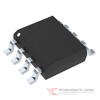
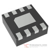
The MC100LVEL51 is available in two package options, each optimized for different application requirements. The SOIC-8 NB package measures 3.94 mm × 3.94 mm with a body height of 1.75 mm, providing a standard surface-mount footprint suitable for conventional printed circuit board assembly processes. The TSSOP-8 package measures 3.00 mm × 3.00 mm with a body height of 0.95 mm, offering a more compact footprint for space-constrained applications.
Thermal management is an important consideration in high-speed digital applications. The MC100LVEL51 in SOIC-8 NB package exhibits a junction-to-ambient thermal resistance (θJA) of 190°C/W at 0 linear feet per minute (Lfpm) airflow and 130°C/W at 500 Lfpm airflow. The junction-to-case thermal resistance (θJC) is 41 to 44°C/W with ±5% tolerance. These thermal parameters allow designers to calculate the junction temperature rise above ambient based on the power dissipation and available cooling.
The MC100LVEL51 in TSSOP-8 package exhibits a junction-to-ambient thermal resistance of 185°C/W at 0 Lfpm airflow and 140°C/W at 500 Lfpm airflow. The junction-to-case thermal resistance is also 41 to 44°C/W. The more compact TSSOP-8 package exhibits slightly higher thermal resistance due to its smaller size, requiring more careful thermal management in high-power applications.
Both packages are Pb-free and RoHS compliant. The SOIC-8 NB package has a moisture sensitivity level of 1, while the TSSOP-8 package has a moisture sensitivity level of 3, requiring 168 hours of dry storage before reflow soldering if the package has been exposed to moisture. The devices meet UL 94 V-0 flammability rating at 0.125 inches thickness with an oxygen index of 28 to 34.
Wave soldering of the MC100LVEL51 should be performed at 260°C for 2 to 3 seconds to ensure proper solder joint formation while minimizing thermal stress on the device. The device incorporates ESD protection exceeding 4 kV for human body model and 200V for machine model, protecting against electrostatic discharge during handling and assembly.
Design Considerations and Application Guidelines for the MC100LVEL51
Proper termination of the MC100LVEL51 outputs is essential for maintaining signal integrity in high-speed applications. The typical termination scheme employs a 50-ohm resistor connected from each output to a termination voltage (VTT) equal to VCC − 3.0V. This termination voltage is approximately midway between the output HIGH and LOW levels, providing optimal impedance matching and reducing reflections on transmission lines.
The MC100LVEL51 is designed to operate with differential clock inputs, allowing the device to function as a negative edge-triggered flip-flop. When implementing differential clock distribution, the CLK and CLK-bar inputs should be driven with equal and opposite signals. The differential input structure with clamp circuitry ensures stable operation even if one input is left open, though this is not recommended for optimal performance.
The asynchronous reset input of the MC100LVEL51 allows system initialization without waiting for clock edges. However, designers must observe the reset recovery time specification to avoid metastability. The reset signal should be released at least 350 picoseconds (maximum specification) before the next active clock edge to ensure reliable operation.
Power supply decoupling is essential for maintaining the performance of the MC100LVEL51. High-frequency bypass capacitors should be placed close to the VCC and VEE pins to minimize supply noise and maintain stable operating conditions. The typical power supply current of 35 mA should be considered when calculating total system power requirements and selecting appropriate power distribution components.
The MC100LVEL51 operates across a temperature range of −40°C to +85°C, with specifications provided at three temperature points. System designers should verify that the application environment remains within this range and consider thermal management strategies if the device will operate near the upper temperature limit.
The device is suitable for applications including clock distribution networks, frequency dividers, phase-locked loop circuits, and general-purpose synchronous logic. The low propagation delay and high toggle frequency make the MC100LVEL51 particularly well-suited for applications where timing precision and speed are important performance factors.
Conclusion
The MC100LVEL51 represents a mature, high-performance differential clock D flip-flop optimized for 3.3V ECL applications. With propagation delays of 475 picoseconds, a maximum toggle frequency of 2.8 GHz, and comprehensive ESD protection, the device delivers the performance required for modern high-speed digital systems. The availability of both LVPECL and LVNECL operating modes provides flexibility in system integration, while the dual package options accommodate different board layout constraints. The MC100LVEL51's temperature-compensated design, low cycle-to-cycle jitter, and robust input structures make it a reliable choice for applications demanding precision clock distribution and data synchronization in the 3.3V operating environment.
Frequently Asked Questions (FAQ)
- Q1. What is the primary functional difference between the MC100LVEL51 and the original EL51 device?
-
- A1. The MC100LVEL51 is functionally equivalent to the EL51 but operates from a 3.3V supply instead of the higher voltage required by the original device. Despite the lower supply voltage, the MC100LVEL51 maintains propagation delays and output transition times essentially equal to the EL51, making it suitable for modern low-voltage applications requiring equivalent performance.
- Q2. Can the MC100LVEL51 be used as a negative edge-triggered flip-flop?
-
- A2. Yes, the differential clock inputs of the MC100LVEL51 allow the device to be configured as a negative edge-triggered flip-flop. By properly utilizing the CLK and CLK-bar differential inputs, designers can implement negative edge triggering, providing flexibility in clock distribution architectures.
- Q3. What happens to the MC100LVEL51 outputs if the differential clock inputs are left open?
-
- A3. The MC100LVEL51 incorporates clamp circuitry that maintains stability under open input conditions. When the CLK input is left open, it is pulled down to VEE, while the CLK-bar input is biased at VCC/2. However, leaving inputs open is not recommended for optimal performance and should be avoided in production designs.
- Q4. What are the two operating modes of the MC100LVEL51, and how do they differ?
-
- A4. The MC100LVEL51 supports LVPECL mode (VCC = 3.3V, VEE = 0V) and LVNECL mode (VCC = 0V, VEE = −3.3V). Both modes deliver identical functional performance and timing characteristics, but the voltage levels and current directions differ. The selection between modes depends on the system's power distribution architecture.
- Q5. What is the significance of the reset recovery time specification for the MC100LVEL51?
-
- A5. Reset recovery time specifies the minimum interval required between the release of the asynchronous reset and the next active clock edge. For the MC100LVEL51, this is 350 picoseconds maximum. Observing this specification prevents metastability issues that could arise if the reset signal is released too close to an active clock edge, ensuring reliable system operation.
- Q6. How should the outputs of the MC100LVEL51 be terminated in high-speed applications?
-
- A6. The typical termination scheme for the MC100LVEL51 employs a 50-ohm resistor connected from each output to a termination voltage (VTT) equal to VCC − 3.0V. This termination voltage is approximately midway between the output HIGH and LOW levels, providing optimal impedance matching and reducing reflections on transmission lines.
- Q7. What is the maximum toggle frequency of the MC100LVEL51, and what does this specification represent?
-
- A7. The maximum toggle frequency of the MC100LVEL51 is 2.8 GHz at 25°C. This specification represents the maximum rate at which the device can switch between states when the D input is held at a fixed level and the clock input receives continuous transitions. This specification is relevant for applications using the MC100LVEL51 as a frequency divider or in phase-locked loop circuits.
- Q8. What are the setup and hold time requirements for the MC100LVEL51?
-
- A8. Setup time is specified at 150 picoseconds, representing the minimum duration the D input must remain stable before a clock edge. Hold time is specified at 200 picoseconds, representing the minimum duration the D input must remain stable after a clock edge. These timing parameters define the data window around the clock edge and are essential for reliable data capture in synchronous systems.
- Q9. What is the cycle-to-cycle jitter specification of the MC100LVEL51, and why is it important?
-
- A9. The cycle-to-cycle jitter of the MC100LVEL51 is specified at 7.0 picoseconds typical, with a range of 6.9 to 7.1 picoseconds across the operating temperature range. Low jitter is important for applications where clock distribution accuracy directly impacts system performance, such as high-speed data converters or precision timing circuits.
- Q10. What are the differences between the SOIC-8 NB and TSSOP-8 package options for the MC100LVEL51?
-
- A10. The SOIC-8 NB package measures 3.94 mm × 3.94 mm with a body height of 1.75 mm, providing a standard surface-mount footprint. The TSSOP-8 package measures 3.00 mm × 3.00 mm with a body height of 0.95 mm, offering a more compact footprint. The TSSOP-8 package has a moisture sensitivity level of 3 (requiring 168 hours of dry storage), while the SOIC-8 NB has a moisture sensitivity level of 1. The TSSOP-8 package exhibits slightly higher thermal resistance due to its smaller size.
- Q11. What power supply decoupling strategy is recommended for the MC100LVEL51?
-
- A11. High-frequency bypass capacitors should be placed close to the VCC and VEE pins to minimize supply noise and maintain stable operating conditions. The typical power supply current of 35 mA should be considered when calculating total system power requirements and selecting appropriate power distribution components.
- Q12. What is the operating temperature range of the MC100LVEL51, and how does temperature affect its performance?
-
- A12. The MC100LVEL51 operates across a temperature range of −40°C to +85°C. The device incorporates temperature compensation circuitry that maintains consistent performance across this range. Specifications are provided at three temperature points (−40°C, +25°C, and +85°C) to allow designers to verify performance at their specific operating conditions.
- Q13. What ESD protection does the MC100LVEL51 provide?
-
- A13. The MC100LVEL51 incorporates ESD protection exceeding 4 kV for human body model and 200V for machine model. This protection guards against electrostatic discharge during handling and assembly, reducing the risk of device damage from static electricity.
- Q14. What is the minimum input signal swing required for the MC100LVEL51 to operate reliably?
-
- A14. The MC100LVEL51 accepts input signal swings ranging from 150 mV to 1000 mV peak-to-peak. The minimum input swing of 150 mV ensures that the device can operate with low-amplitude differential signals, while the maximum swing of 1000 mV accommodates higher-amplitude signals without saturation or distortion.
- Q15. What are the typical applications for the MC100LVEL51?
-
- A15. The MC100LVEL51 is suitable for applications including clock distribution networks, frequency dividers, phase-locked loop circuits, and general-purpose synchronous logic. The low propagation delay and high toggle frequency make the MC100LVEL51 particularly well-suited for applications where timing precision and speed are important performance factors.