Product Overview of the AD8504 Micropower CMOS Operational Amplifier
The AD8504 is a low-power, precision CMOS operational amplifier manufactured by Analog Devices Inc., designed specifically for applications where power consumption must be minimized without compromising signal processing quality. This device represents a significant advancement in micropower amplifier technology, delivering a maximum supply current of just 1 microampere per amplifier while maintaining precision specifications suitable for demanding measurement and signal conditioning tasks.
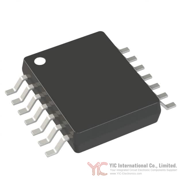
The AD8504 integrates four independent operational amplifier circuits within a single 14-lead TSSOP surface-mount package, making it an efficient solution for multi-channel signal processing in space-constrained designs. The quad-channel architecture allows designers to implement complex signal conditioning, filtering, and detection functions while maintaining the ultra-low power consumption profile that distinguishes this device from conventional operational amplifiers.
Core Performance Characteristics of the AD8504 Series
The AD8504 achieves its micropower operation through advanced CMOS circuit design while maintaining precision specifications that rival higher-power alternatives. The maximum input offset voltage of 3 millivolts ensures accurate signal representation across the operating range, while the typical input bias current of 1 picoampere minimizes loading effects on high-impedance signal sources. These characteristics combine to deliver precision signal processing without the need for system calibration, reducing design complexity and time-to-market for end applications.
The device operates with unity gain stability, meaning it can be configured as a unity-gain buffer or follower without requiring frequency compensation networks. This simplifies circuit design and reduces component count, particularly valuable in portable applications where board space and power budget are constrained. The no phase reversal characteristic ensures predictable behavior in feedback configurations, allowing designers to implement stable control loops and signal processing chains with confidence.
Supply Voltage Flexibility and Operating Range of the AD8504
The AD8504 accommodates both single-supply and dual-supply configurations, providing design flexibility across diverse application requirements. In single-supply mode, the device operates from +1.8 volts to +5.5 volts, enabling integration into modern low-voltage battery-powered systems. The dual-supply option ranges from ±0.9 volts to ±2.75 volts, supporting applications requiring bipolar signal processing or symmetric supply architectures.
This voltage flexibility proves particularly valuable in portable equipment where battery voltage naturally decreases as the cell discharges. The AD8504 maintains specified performance across its entire supply voltage range, ensuring consistent signal processing quality throughout the battery's operational life. The ability to operate at supply voltages as low as 1.8 volts positions the device for integration into next-generation ultra-low-power systems, including wearable medical devices and energy-harvesting applications.
The supply current remains remarkably stable across the operating voltage range, with typical values remaining near the 1-microampere specification even as supply voltage varies. This consistency simplifies power budget calculations and enables accurate prediction of battery life in portable applications. Performance characteristics remain well-controlled across the industrial temperature range of -40°C to +85°C, with extended specifications available for -40°C to +125°C operation in demanding environments.
Input and Output Characteristics of the AD8504
The AD8504 implements rail-to-rail input and output operation, a feature that maximizes the dynamic range available for signal processing. Rail-to-rail input capability means the common-mode input voltage can extend from ground (or the negative supply in dual-supply configurations) to the positive supply rail, allowing the device to process signals across the full supply voltage span without requiring input biasing networks. This characteristic proves particularly valuable in low-voltage systems where every millivolt of dynamic range contributes meaningfully to signal-to-noise ratio and measurement resolution.
Rail-to-rail output operation ensures the amplifier can swing its output voltage from near ground potential to near the positive supply rail, maximizing the available output signal swing. In low-voltage applications, this capability becomes critical for achieving adequate signal levels without requiring additional output buffering or level-shifting circuitry. The combination of rail-to-rail input and output characteristics allows designers to implement high-gain signal conditioning stages in single-supply systems without the complexity traditionally required for low-voltage operation.
The input bias current remains exceptionally low across the common-mode input voltage range, maintaining the 1-picoampere specification even as the input voltage approaches the supply rails. This consistency ensures predictable circuit behavior in high-impedance sensor applications, where input bias current can introduce significant errors if not carefully managed. The output saturation voltage characteristics demonstrate the device's ability to deliver useful signal levels even when driving moderate load currents, with saturation voltage remaining well-controlled across the temperature range.
Precision and Accuracy Features of the AD8504
The AD8504 achieves its precision specifications through careful circuit design and manufacturing process control. The maximum input offset voltage of 3 millivolts represents the maximum deviation from ideal zero-input-zero-output behavior, a specification that directly impacts the accuracy of precision measurement systems. The offset voltage distribution across production units shows tight clustering around the nominal value, indicating consistent manufacturing quality and predictable device-to-device performance.
The input offset voltage temperature coefficient, specified at typical values well below 10 microvolts per degree Celsius, ensures that temperature variations in the operating environment produce minimal changes in amplifier offset. This stability proves particularly valuable in portable applications where ambient temperature may fluctuate significantly, such as outdoor environmental monitoring or wearable medical devices. The offset voltage remains stable across the common-mode input voltage range, eliminating the need for input-dependent calibration adjustments.
The common-mode rejection ratio (CMRR) exceeds 80 decibels across the audio frequency range, providing strong rejection of common-mode interference signals that appear equally on both amplifier inputs. This characteristic proves valuable in sensor applications where differential signal levels may be small compared to common-mode noise from power supply ripple or electromagnetic interference. The power supply rejection ratio (PSRR) similarly exceeds 80 decibels, ensuring that supply voltage variations produce minimal changes in amplifier output, a critical requirement in battery-powered systems where supply voltage naturally decreases over time.
Thermal Management and Reliability of the AD8504
The AD8504 in its 14-lead TSSOP package exhibits thermal resistance characteristics suitable for surface-mount assembly on standard printed circuit boards. The junction-to-ambient thermal resistance remains low enough to allow continuous operation at rated specifications without requiring heat sinks or forced-air cooling, a significant advantage in portable applications where thermal management complexity must be minimized.
The device is fully specified over the industrial temperature range of -40°C to +85°C, with extended specifications available for operation to +125°C. This temperature range coverage enables deployment in diverse environments, from consumer portable equipment operating in controlled indoor conditions to industrial remote sensors exposed to extreme ambient temperatures. The thermal characteristics remain predictable across this range, allowing designers to implement temperature-compensated circuits if application requirements demand temperature-independent performance.
The AD8504 incorporates electrostatic discharge (ESD) protection circuitry to safeguard against damage during handling and assembly. While this protection provides a baseline level of ESD immunity, proper ESD precautions should be maintained throughout the manufacturing and assembly process to ensure device reliability and prevent performance degradation. The device's CMOS construction inherently provides good ESD immunity compared to bipolar alternatives, reducing the risk of damage from typical handling scenarios.
Packaging and Integration Options for the AD8504
The AD8504 is available in a 14-lead TSSOP surface-mount package, a standard form factor widely supported by modern assembly equipment and compatible with high-density printed circuit board designs. The TSSOP package provides excellent thermal characteristics for a surface-mount device while maintaining a compact footprint suitable for portable applications. The package dimensions comply with JEDEC standards, ensuring compatibility with industry-standard assembly processes and solder reflow profiles.
The quad-channel integration within a single package provides significant advantages for multi-channel applications. Rather than requiring four separate dual-channel devices or eight individual single-channel amplifiers, the AD8504 consolidates four complete amplifier circuits into a single component. This integration reduces board area, simplifies routing, and decreases the overall component count, all factors that contribute to lower manufacturing costs and improved reliability through reduced solder joint count.
The 14-lead TSSOP package includes dedicated supply pins for each amplifier pair, allowing independent biasing and supply decoupling if application requirements demand isolation between channels. This flexibility supports applications where different channels operate at different supply voltages or require independent power management. The compact package dimensions make the AD8504 suitable for integration into space-constrained portable devices, including wearable sensors and handheld measurement instruments.
Application Scenarios for the AD8504 in Portable and Remote Systems
The AD8504's combination of micropower operation, precision specifications, and rail-to-rail characteristics makes it well-suited for diverse portable and remote sensing applications. In portable medical equipment such as bedside monitors and pulse oximeters, the AD8504 provides precision signal conditioning for physiological sensors while minimizing power consumption to extend battery life. The low input bias current proves particularly valuable in these applications, where sensor impedance may be high and input bias current-induced errors must be minimized.
Glucose meters and other point-of-care diagnostic devices benefit from the AD8504's ability to process small sensor signals with high precision while operating from battery supplies. The rail-to-rail input and output characteristics allow these devices to extract maximum signal information from miniature sensors, improving measurement resolution and diagnostic accuracy. The micropower operation extends battery life between charging cycles, a critical requirement for devices intended for frequent use throughout the day.
Remote environmental monitoring systems, including temperature and humidity sensors deployed in inaccessible locations, rely on the AD8504's low power consumption to achieve extended operational life from primary batteries or energy-harvesting sources. The device's ability to operate from supply voltages as low as 1.8 volts enables integration with modern low-power wireless transceivers, creating complete sensor nodes that can operate for months or years on a single battery charge.
Smoke and fire detection systems utilize the AD8504 for signal conditioning from photodiode sensors and thermal sensors. The precision offset voltage specification ensures accurate threshold detection, while the low power consumption allows these safety-critical devices to operate continuously without excessive battery drain. Vibration monitoring systems similarly benefit from the AD8504's precision and low power characteristics, enabling condition-based maintenance systems that detect equipment degradation before failure occurs.
Current sensing applications leverage the AD8504's low input bias current and precision offset voltage to implement accurate current measurement circuits. The device can be configured as a transimpedance amplifier to convert small currents from current-sensing resistors into measurable voltage signals, with the low offset voltage ensuring accurate measurement of small currents without requiring calibration. Low-power filter applications utilize the AD8504's unity-gain stability and precision characteristics to implement active filtering stages that condition sensor signals before analog-to-digital conversion.
Conclusion
The AD8504 represents a mature solution for applications requiring precision signal processing with minimal power consumption. The combination of 1-microampere supply current, 3-millivolt maximum offset voltage, and rail-to-rail input and output operation addresses the core requirements of modern portable and remote sensing systems. The quad-channel integration within a compact TSSOP package provides efficient implementation of multi-channel signal conditioning, while the flexible supply voltage range accommodates diverse system architectures. The device's proven performance across the industrial temperature range and its availability in standard surface-mount packaging make it a practical choice for production applications requiring reliable, low-power signal processing.
Frequently Asked Questions (FAQ)
- Q1. What is the primary advantage of the AD8504's 1-microampere supply current specification compared to conventional operational amplifiers?
-
- A1. The 1-microampere supply current per amplifier enables extended battery life in portable applications. For example, a portable device powered by a 100-milliampere-hour battery could theoretically operate for over 100,000 hours (approximately 11 years) if the AD8504 were the only current-consuming component. While real applications consume additional current for sensors, signal processing, and wireless transmission, the AD8504's micropower operation significantly extends battery life compared to conventional amplifiers that typically consume milliamperes per channel.
- Q2. How does the rail-to-rail input and output capability improve performance in low-voltage applications?
-
- A2. Rail-to-rail operation maximizes the available signal swing in low-voltage systems. In a 1.8-volt single-supply system, a conventional amplifier might limit input signals to a 0.5-volt to 1.3-volt range, wasting 0.2 volts of headroom at each rail. The AD8504 can process signals from near ground to near the positive supply rail, utilizing the full 1.8-volt span. This expanded dynamic range improves signal-to-noise ratio and measurement resolution, allowing smaller sensor signals to be processed without additional amplification stages.
- Q3. Can the AD8504 be used in applications requiring both single-supply and dual-supply operation?
-
- A3. Yes, the AD8504 supports both configurations. Single-supply operation from +1.8V to +5.5V suits battery-powered portable devices, while dual-supply operation from ±0.9V to ±2.75V supports applications requiring bipolar signal processing or symmetric supply architectures. The same device can be configured for either mode by adjusting the power supply connections and biasing networks, providing design flexibility across different application requirements.
- Q4. What does the "no phase reversal" characteristic mean, and why is it important?
-
- A4. No phase reversal means the amplifier output maintains the correct polarity relationship with the input signal across all operating conditions. In some amplifier designs, if the input signal exceeds certain limits or supply voltage drops below a threshold, the output can invert unexpectedly. The AD8504 guarantees this won't occur, ensuring predictable behavior in feedback circuits and signal processing chains. This characteristic is particularly important in control systems and threshold detectors where output polarity errors could cause system malfunction.
- Q5. How does the 3-millivolt maximum offset voltage specification impact system design?
-
- A5. The offset voltage represents the input voltage that would produce zero output voltage in an ideal amplifier. With a 3-millivolt maximum offset, a gain-of-100 amplifier stage could produce up to 300 millivolts of output error with zero input signal. In precision measurement applications, this offset must be accounted for through calibration or offset cancellation circuits. The tight offset voltage distribution across production units and its stability across temperature and supply voltage variations allow designers to implement predictable offset compensation without requiring individual device calibration.
- Q6. What is the significance of the 1-picoampere input bias current specification?
-
- A6. Input bias current represents the small current that flows into the amplifier inputs. At 1 picoampere, this current is negligible in most applications, but becomes significant when interfacing with very high-impedance sensors. For example, a 1-gigaohm sensor impedance would produce only 1 millivolt of error voltage from the 1-picoampere bias current. This low bias current eliminates the need for input buffering or bias current compensation in high-impedance applications, simplifying circuit design and reducing component count.
- Q7. How should the AD8504 be protected from electrostatic discharge during handling and assembly?
-
- A7. Although the AD8504 includes ESD protection circuitry, proper ESD precautions should be maintained throughout manufacturing and assembly. This includes using grounded work surfaces, ESD-safe handling tools, and antistatic wrist straps when handling devices. Components should be stored in antistatic bags or conductive foam, and assembly equipment should be properly grounded. While the CMOS construction provides inherent ESD immunity superior to bipolar alternatives, these precautions prevent potential damage that could degrade device performance or cause latent failures.
- Q8. What thermal considerations apply when using the AD8504 in high-temperature environments?
-
- A8. The AD8504 is specified for operation to +85°C (industrial range) or +125°C (extended range), with performance characteristics remaining well-controlled across these ranges. The thermal resistance of the TSSOP package is low enough that continuous operation at rated specifications requires no heat sinking. However, designers should verify that the actual junction temperature remains within specification by calculating power dissipation and accounting for ambient temperature and board thermal characteristics. In applications approaching the maximum temperature limit, thermal simulation or testing should confirm adequate margin.
- Q9. How does the common-mode rejection ratio (CMRR) specification of 80 decibels affect noise immunity?
-
- A9. An 80-decibel CMRR means that common-mode signals (noise appearing equally on both inputs) are attenuated by a factor of 10,000 compared to differential signals. If a 1-volt power supply ripple appears on both amplifier inputs, the CMRR specification guarantees that this noise contributes less than 0.1 millivolts to the output. This strong rejection of common-mode interference proves valuable in sensor applications where differential signal levels may be small compared to environmental noise, allowing accurate measurement without requiring extensive shielding or filtering.
- Q10. What is the practical difference between the AD8504 and the AD8502 mentioned in the datasheet?
-
- A10. The AD8502 is a dual-channel version (two amplifiers) available in an 8-lead SOT-23 package, while the AD8504 is a quad-channel version (four amplifiers) in a 14-lead TSSOP package. Both devices share identical electrical specifications and performance characteristics. The choice between them depends on application requirements: the AD8502 suits applications requiring only two channels or where the smaller SOT-23 package is preferred, while the AD8504 provides more channels in a slightly larger package, offering better integration for multi-channel applications.
- Q11. Can the AD8504 be used for precision current measurement applications?
-
- A11. Yes, the AD8504 is well-suited for current sensing through transimpedance amplifier configurations. A current-sensing resistor converts the measured current into a proportional voltage, which the AD8504 amplifies with high precision. The low input bias current ensures minimal loading on the sensing resistor, while the low offset voltage enables accurate measurement of small currents without calibration. For example, measuring 1-milliampere through a 1-kilohm sensing resistor produces 1 volt, which can be amplified to a convenient measurement range with minimal error.
- Q12. How does the unity-gain stability characteristic simplify circuit design?
-
- A12. Unity-gain stability means the amplifier can be configured as a buffer (unity-gain follower) without requiring frequency compensation networks. Conventional amplifiers often require compensation capacitors to prevent oscillation in unity-gain configurations, adding component count and design complexity. The AD8504 eliminates this requirement, allowing direct implementation of high-impedance buffers, voltage followers, and unity-gain summing amplifiers without additional components. This simplification reduces board area and cost while improving reliability through reduced component count.