- English
-
EnglishDeutschItaliaFrançais한국의русскийSvenskaNederlandespañolPortuguêspolski繁体中文SuomiGaeilgeSlovenskáSlovenijaČeštinaMelayuMagyarországHrvatskaDanskromânescIndonesiaΕλλάδαБългарски езикGalegolietuviųMaoriRepublika e ShqipërisëالعربيةአማርኛAzərbaycanEesti VabariikEuskeraБеларусьLëtzebuergeschAyitiAfrikaansBosnaíslenskaCambodiaမြန်မာМонголулсМакедонскиmalaɡasʲພາສາລາວKurdîსაქართველოIsiXhosaفارسیisiZuluPilipinoසිංහලTürk diliTiếng ViệtहिंदीТоҷикӣاردوภาษาไทยO'zbekKongeriketবাংলা ভাষারChicheŵaSamoa日本語SesothoCрпскиKiswahiliУкраїнаनेपालीעִבְרִיתپښتوКыргыз тилиҚазақшаCatalàCorsaLatviešuHausaગુજરાતીಕನ್ನಡkannaḍaमराठी
Your Guide to Semiconductor Materials: Types, Traits, and Technologies
Catalog

Overview of Semiconductor Materials
Materials are categorized based on their electrical conductivity into three broad groups: conductors, semiconductors, and insulators. Semiconductors are intriguing due to their resistivity spanning from 1 mΩ·cm to 1 GΩ·cm, and they demonstrate an increase in conductance with rising temperatures, a behavior quite distinct from metals. Their remarkable sensitivity to external factors; light, heat, magnetic fields, and electric forces, gives rise to unique physical effects, underpinning the diversity of their properties. The ability of semiconductors to adapt and respond to these stimuli fuels their role in solid-state electronic devices, unlocking a multitude of functionalities across various types. This adaptability paves the way for breakthroughs in technology, prominently in devices like transistors and solar cells, where mastery over electron flow elevates functionality.
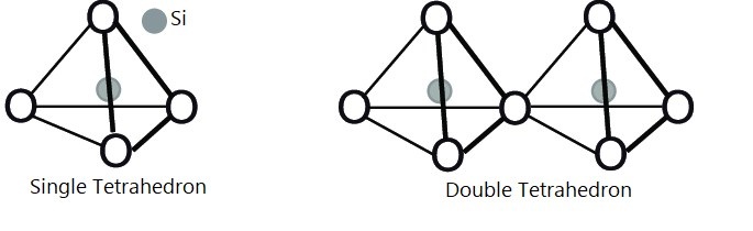
Semiconductors are distinguished by their saturated covalent bonds, forming complex structures like diamond or sphalerite lattices. Historically, materials such as Galena (PbS) and cuprous oxide (Cu2O) are pioneers in semiconductor discovery. Elemental semiconductors, such as silicon, germanium, and selenium, have been instrumental in technological progress. Notably, silicon has facilitated the evolution of integrated circuits, fostering innovation and propelling research into III-V compounds, for instance, gallium arsenide (GaAs), which is ideal for microwave and optoelectronic applications. The deliberate application of silicon and related materials in semiconductor tech has redefined communication and computation, emphasizing how material properties can drive technological evolution. As practical use and research continue to push the limits of what semiconductors can achieve, a dynamic environment emerges where science meets practical application, propelling modern electronics forward.
Categorization of Semiconductor Materials
Semiconductor materials can be categorized based on their chemical composition and structure into elemental, compound (inorganic and organic), amorphous, and liquid types. This classification highlights the wide range of materials used in semiconductor technology and their role in enabling diverse applications.Elemental Semiconductors
Elemental semiconductors mainly come from group IV of the periodic table, with silicon and germanium being the most important examples. These materials are valued for their stability, availability, and reliable performance. Silicon, in particular, is the backbone of modern integrated circuits and microprocessors, shaping much of today’s electronic innovation. Germanium, once central to early transistor technology, still finds use in specialized high-speed and optical applications.Compound Semiconductors
Compound semiconductors are formed by combining elements from different groups of the periodic table.• Inorganic Compounds: These include binary compounds such as GaAs (III-V) and SiC (IV-IV), widely used in LEDs, laser diodes, and high-frequency devices. More complex materials like ternary (e.g., CuGaSe₂) and quaternary compounds offer tunable properties for tailored applications in optoelectronics and photovoltaics.
• Organic Compounds: Some organic materials, such as naphthalene derivatives, exhibit semiconducting behavior. While still largely in research and development, organic semiconductors show promise in flexible, lightweight, and low-cost electronics, such as OLED displays and solar cells.
Non-Crystalline and Liquid Semiconductors
Not all semiconductors are crystalline. Amorphous semiconductors, such as amorphous silicon, are used in thin-film transistors and solar cells due to their ease of large-area deposition. Liquid semiconductors, though mainly explored in research, have potential in optoelectronic applications. Their unique properties continue to inspire studies into unconventional device designs.Properties of Semiconductor Materials
Performance Attributes
Semiconductors exhibit a variety of attributes, such as resistivity, bandgap, carrier mobility, non-equilibrium carrier lifetime, and dislocation density. These aspects are fundamental in shaping how semiconductors function and influence device designs. These properties are carefully balanced to meet specific functions. Collaborative efforts across various fields help develop solutions that address current needs and adapt to future changes in technology.
Evaluation of Device Capabilities
• Characteristics of Transistors
Transistors benefit tremendously from increased carrier mobility and prolonged non-equilibrium carrier longevity, enhancing frequency and quick response times. When operating under high temperatures, large bandgaps become instrumental. For faster and more stable devices leads to constant exploration of new materials and methods. This work recognizes the careful balance needed to achieve the right features for top performance.
• Essentials for Optoelectronic Devices
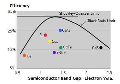
Optoelectronic devices, like detectors and solar cells, rely heavily on extended non-equilibrium carrier lifetimes and optimal bandgaps to improve detector sensitivity and solar cell efficiency. Designing these devices entails a skillful selection and arrangement of materials, informed by practical experience and extensive testing, all aimed at maximizing absorption and effective light conversion.
• Efficiency in Thermoelectric Devices
Thermoelectric devices harness efficiency through pronounced temperature gradients and materials possessing beneficial bandgaps and conductivities. Realizing the full potential of these devices demands a fusion of scholarly insight and industrial know-how, showing the harmonious relationship between understanding and practical application. Ongoing work focuses on improving these materials, with the understanding that even small changes can lead to meaningful progress in energy conversion systems.
Progression in Semiconductor Material Technology
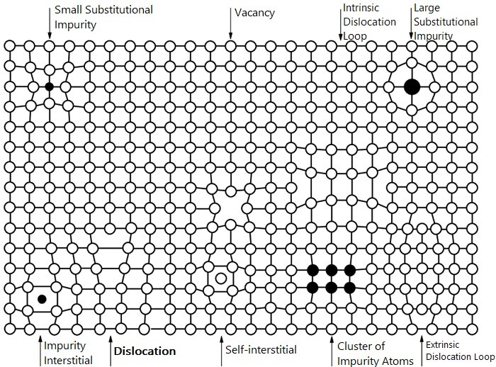
In the field of semiconductor innovation, the mastery of impurity atom regulation and crystal defect management holds transformative potential, as these factors distinctly alter the electronic characteristics of materials. A methodical strategy that delves into the intricacies of purification and astute defect control lays the groundwork for advancements in material science. This involves a symphony of detailed methodologies, encompassing both cutting-edge chemical and physical purification processes, along with state-of-the-art thin-film epitaxial growth techniques, collectively steering the course towards technological breakthroughs.
Purification Processes
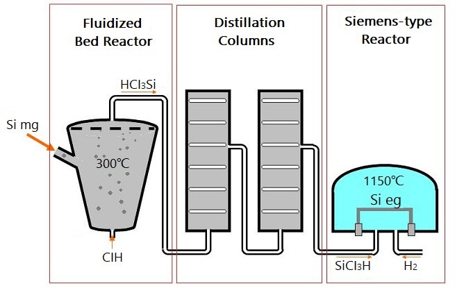
The role of purification in the semiconductor manufacturing process centers around reducing impurity levels to minuscule traces. The utilization of techniques such as zone refining, electron beam melting, and gas phase purification has achieved unprecedented silicon and germanium purity. These methods, through years of enhancement, now permit the fabrication of materials with impurity concentrations quantified in parts per billion. Such refined approaches translate into tangible benefits in electronics manufacturing, where the steadfast consistency and reliability of high-purity materials are mirrored in the longevity and efficiency of electronic devices.
Thin-film Creation
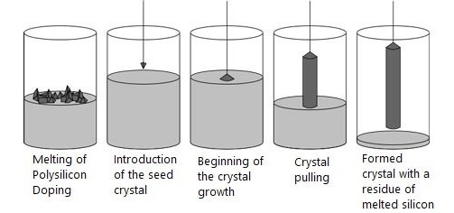
Advanced thin-film epitaxial growth techniques, including Molecular Beam Epitaxy (MBE), Chemical Vapor Deposition (CVD), and Pulsed Laser Deposition (PLD), have charted new territories in microstructural innovation. Alongside classical methods like the Czochralski process and magnetron sputtering, these techniques facilitate the precise formation of uniform single crystals. Epitaxial growth extends the horizons of semiconductor applications in cutting-edge fields such as quantum computing and high-frequency transistors and supports the crafting of multilayered structures with novel properties. Practical applications shows how these techniques bolster computational efficiency and minimize material waste, thus paving the way for sustainable technological evolution.
The extensive perspective on semiconductor material technology exposes a tapestry where purification and epitaxial growth meld into a cohesive fabric of interconnected technologies, together sculpting the future. The continuous enhancement of these methods is a testament not merely to technical skill but also to a deep-seated anticipation of the trajectory of electronics development.
Characteristics of the Semiconductor Material Industry
Expansive Reach
The semiconductor material industry is a vast sector, noted not only for its impressive financial footprint but also for its significant impact across various technology-driven fields. This industry fuels innovations in artificial intelligence, telecommunications, and consumer electronics, forming the backbone of the technological infrastructure that shapes contemporary life. As nations vie for a stronger foothold in the tech world, strategic investments and international alliances become instrumental in amplifying their influence and reach.
Diverse Product Landscape
The semiconductor industry is intricately segmented, housing an array of product categories aimed at fulfilling distinct industrial needs. Products range from silicon wafers to compound semiconductors, each contributing uniquely to the broader ecosystem of technological utility. Such segmentation encourages specialized innovation and spurs the growth of niche markets, enabling custom applications to flourish. Collaboration across different fields helps move beyond old boundaries, creating new ideas and progress that push the industry forward.
Precision in Production
Creating semiconductor materials demands adherence to strict purity benchmarks and complex technical protocols. The constant drive for accuracy in production hinges on sophisticated methods that assure the quality and dependability of materials. Institutions engage in extensive research and integrate state-of-the-art technology to navigate these high standards. Consistent upgrades to equipment and process refinements lead to the production of materials that honor the critical demands of microelectronics, securing a competitive edge in a rapidly evolving technological landscape.
Economic Viability
While the industry commands sizable dimensions, individual material costs are kept manageable, reflecting a dedication to cost-efficient production. This is achieved through manufacturing processes that cleverly strike a balance between massive output and quality, simultaneously maximizing production while curtailing costs. Continuous improvements in resource management and supply chain strategies are part of ongoing efforts to further reduce expenses. These measures fortify the industry’s established legacy of delivering top-tier materials at attractive price points.
Conclusion
Semiconductors continue to power innovation through their versatile properties and expanding applications. Advancements in purification and epitaxial growth methods have raised material quality, while global demand fuels industry growth across sectors. As research and manufacturing evolve, semiconductor materials will remain a driving force behind technological breakthroughs and the future of connected, intelligent systems.
Related Blog
-
How Many Zeros in a Million, Billion, Trillion?
![How Many Zeros in a Million, Billion, Trillion?]()
July 29th, 2024
Million represents 106, an easily graspable figure when compared to everyday items or annual salaries. Billion, equivalent to 109, starts to stretch t... -
IRLZ44N MOSFET Datasheet, Circuit, Equivalent, Pinout
![IRLZ44N MOSFET Datasheet, Circuit, Equivalent, Pinout]()
August 28th, 2024
The IRLZ44N is a widely-used N-Channel Power MOSFET. Renowned for its excellent switching capabilities, it is highly suited for numerous applications,... -
Battery Temperature Too Low, Charging Stopped. How to Fix It?
![Battery Temperature Too Low, Charging Stopped. How to Fix It?]()
October 6th, 2024
Mobile phone battery charging issues are common but can be effectively managed. Temperature plays a big role in battery efficiency, as smartphone batt... -
BC547 Transistor Comprehensive Guide
![BC547 Transistor Comprehensive Guide]()
July 4th, 2024
The BC547 transistor is commonly used in a variety of electronic applications, ranging from basic signal amplifiers to complex oscillator circuits and... -
Comprehensive Guide to SCR (Silicon Controlled Rectifier)
![Comprehensive Guide to SCR (Silicon Controlled Rectifier)]()
April 22th, 2024
Silicon Controlled Rectifiers (SCR), or thyristors, play a pivotal role in power electronics technology because of their performance and reliability. ... -
LR621, SR621SW, 364, AG1 Battery Equivalents and Replacements
![LR621, SR621SW, 364, AG1 Battery Equivalents and Replacements]()
July 15th, 2024
LR621 and SR621SW button batteries are prevalent in compact electronic devices like watches, small toys, calculators, and remote keys. Multiple manufa... -
Fundamentals of Op-Amp Circuits
![Fundamentals of Op-Amp Circuits]()
December 28th, 2023
In the intricate world of electronics, a journey into its mysteries invariably leads us to a kaleidoscope of circuit components, both exquisite and co... -
Comparing NMOS and PMOS Differences and Applications
![Comparing NMOS and PMOS Differences and Applications]()
November 15th, 2024
Understanding the differences between NMOS and PMOS transistors is important in designing efficient circuits. NMOS (N-type Metal-Oxide-Semiconductor) ... -
A Complete Guide to Multiplexers and Their Role in Digital Systems
![A Complete Guide to Multiplexers and Their Role in Digital Systems]()
September 20th, 2025
Multiplexers are components in digital systems, designed to channel multiple input signals into a single output line using binary logic and control si... -
What Do STD, AGM, and Gel Mean On a Battery Charger
![What Do STD, AGM, and Gel Mean On a Battery Charger]()
July 10th, 2024
Traditional lead-acid battery chargers are known for their simplicity and reliability. They have been serving their purpose effectively for years, lar...


Hot Parts
- AS339GTR-G1
- KHU-17D11-24
- LMV751M5/NOPB
- VI-224-MY
- VI-J60-CX-01
- GRM0335C2A6R1DA01J
- LMSP33CB-465
- C1206C222KCRACTU
- GRM1886P2A270JZ01D
- TAJD225M050HNJ
- 08051A471GAT2A
- TLC542IFNR
- DP83848EVV/VCE
- BS62LV4006EIG-70
- GD32F130C8T6
- MC74HC595ADG
- KM68512LG-7
- T491V157M006AT
- ATMEGA8A-AU
- 2SK1086
- NPCE985CAODX
- 74ABT374CMSA
- SN74LVC2G34DCK
- TPSF107M016R0150
- LH28F128BFHBD-PWT2Z1
- G524B3P81U
- M24C04-RDW
- SMM665BFT-546L
- DM9161EP
- 08055C273KAJ2A
- RT0402BRE07124RL
- 0805YA332JAT2A
- T491A106K016AH
- GRM2166P1H750JZ01D
- AD7476AAKSZ-REEL7
- MC908GT16CFBE
- 1812HA820KAT1A
- T491B226M020AT4280
- T491D107K016AT7280
- T491X226M035ATAU04
- IPD60R600P7SAUMA1
- TLP266J(TPL,E
- VI-J31-IZ
- BCM57810SB0KFSBG
- SPC5601PEMLL6
- S29AL016D70MFI013
- R5F5630LJDFP#V0
- VSC8262QR
- LTC4266CCUHF#TRPBF
- 524352471