- English
-
EnglishDeutschItaliaFrançais한국의русскийSvenskaNederlandespañolPortuguêspolski繁体中文SuomiGaeilgeSlovenskáSlovenijaČeštinaMelayuMagyarországHrvatskaDanskromânescIndonesiaΕλλάδαБългарски езикGalegolietuviųMaoriRepublika e ShqipërisëالعربيةአማርኛAzərbaycanEesti VabariikEuskeraБеларусьLëtzebuergeschAyitiAfrikaansBosnaíslenskaCambodiaမြန်မာМонголулсМакедонскиmalaɡasʲພາສາລາວKurdîსაქართველოIsiXhosaفارسیisiZuluPilipinoසිංහලTürk diliTiếng ViệtहिंदीТоҷикӣاردوภาษาไทยO'zbekKongeriketবাংলা ভাষারChicheŵaSamoa日本語SesothoCрпскиKiswahiliУкраїнаनेपालीעִבְרִיתپښتوКыргыз тилиҚазақшаCatalàCorsaLatviešuHausaગુજરાતીಕನ್ನಡkannaḍaमराठी
Bipolar Junction Transistors Work, Symbols, Configurations, and Uses
Catalog
Bipolar Junction Transistors (BJT)
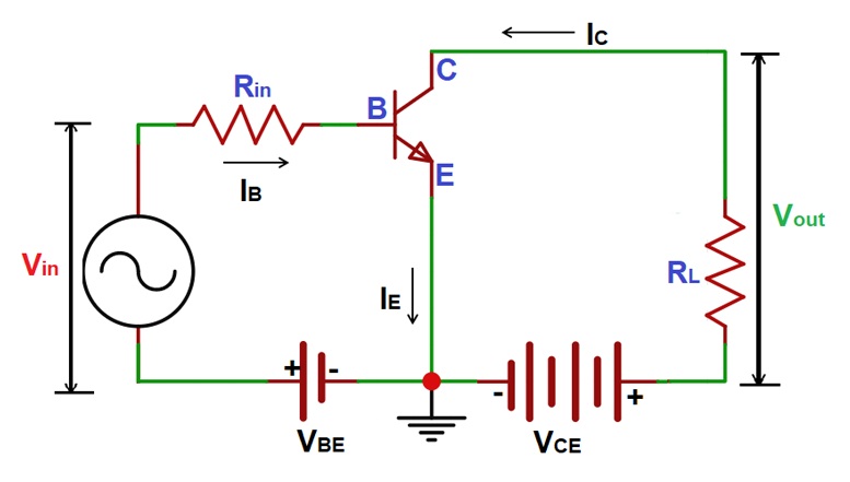
Bipolar Junction Transistors (BJTs) have roles such as electronically controlled switches or amplifiers. These devices, with their distinct three terminals; emitter, base, and collector, adeptly control current flow. They guide electricity from the emitter to the collector, with the base input modulating this process. Much like managing light with a switch, BJTs facilitate sophisticated electronic signal management without physical intervention. Their role in circuits is emphasized by their ability to automate and enable intricate electrical designs, allowing for creative and efficient engineering solutions.
The core of BJT functionality is the meticulous control of electron flow between the emitter and collector. Essentially, a small input current at the base regulates a larger current between the emitter and collector. This allows BJTs to amplify signals or act effectively as switches. BJTs are widely used to raise weak signals to practical levels. This ability supports clearer and more reliable operation in electronic communication systems.
BJT applications span from simple linear amplifiers to advanced switching regulators. Performance depends strongly on how semiconductor materials respond under varying conditions. Careful control of biasing and stabilization improves operation and extends practical limits. Adjustments matched to specific operating conditions often lead to better circuit function and higher reliability.
An in-depth comprehension of BJTs paves the way for designing innovative electronic structures. The capability of the device to operate across low to high-power applications emphasizes its adaptability and significance. This extensive range is beneficial in diverse sectors, including telecommunications and automotive industries.
BJT Symbols and Structure
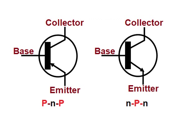
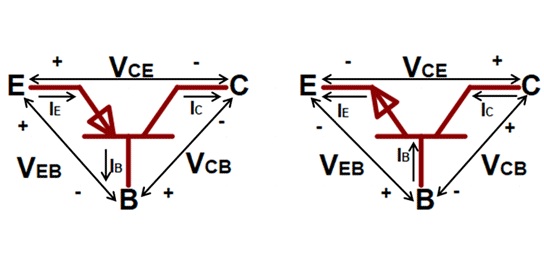
A bipolar junction transistor, or BJT, is identified in circuit diagrams by a standard symbol that shows its three terminals, the base, collector, and emitter. There are two main BJT types, PNP and NPN, and each uses a distinct symbol to indicate its operating behavior.
The key difference between the PNP and NPN symbols is the arrow on the emitter. This arrow shows the direction of conventional current at the emitter terminal. In a PNP transistor, the arrow points toward the base. In an NPN transistor, the arrow points away from the base. This simple arrow direction makes it easy to recognize the transistor type when reading a schematic.
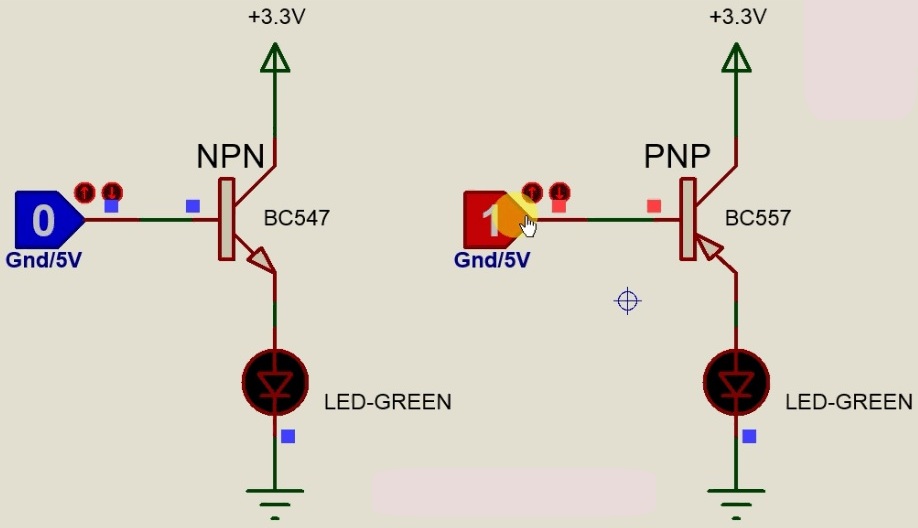
This distinction also appears in basic switching circuits. An NPN transistor is commonly arranged to control current from a load down to ground. A PNP transistor is often arranged to control current from the supply down into the load. These examples show how transistor type affects circuit placement and how the base control signal is applied.
Another practical difference is the way each transistor type is turned on. In typical circuits, an NPN transistor conducts when the base voltage is slightly higher than the emitter voltage. A PNP transistor conducts when the base voltage is slightly lower than the emitter voltage. This explains why NPN and PNP circuits often look opposite in wiring and control logic.
Construction of Bipolar Junction Transistor
![Construction of PNP and NPN Layers]](/upfile/images/bf/20260106085757593.jpg)
A BJT is built from three semiconductor regions that form two junctions. A PNP transistor uses two P-type regions with one N-type region between them. An NPN transistor uses two N-type regions with one P-type region in the center. Each region connects directly to one of the transistor terminals.
The outer regions form the collector and the emitter, while the center region forms the base. The base is made very thin compared with the other regions. This design allows a small base signal to control a much larger current flowing between the collector and emitter.
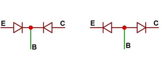
The internal structure of a BJT can be explained using a simple two-diode analogy. Inside the transistor are two junctions that behave like two diodes connected at the base region. This explains why both the base emitter path and the base collector path act like diode junctions under forward bias.
In a PNP transistor, the diode polarities match the PNP layer arrangement. In an NPN transistor, the diode polarities are reversed to match the NPN structure. This analogy helps clarify how the base interacts with the emitter and collector, and how proper biasing determines whether the transistor is off, partially on, or fully on.
Fundamentals of BJT Operation
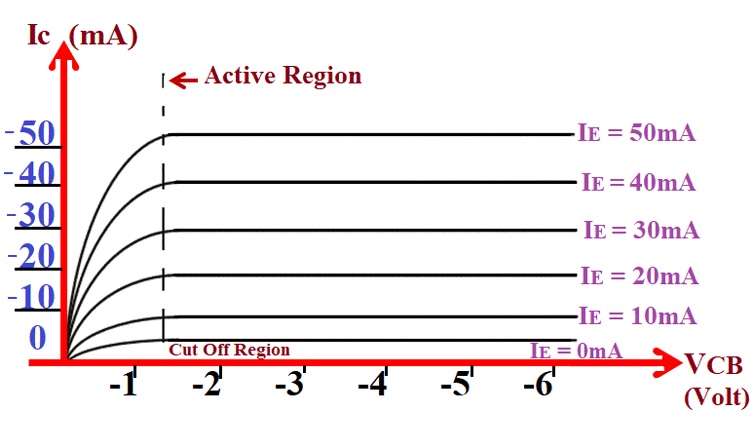
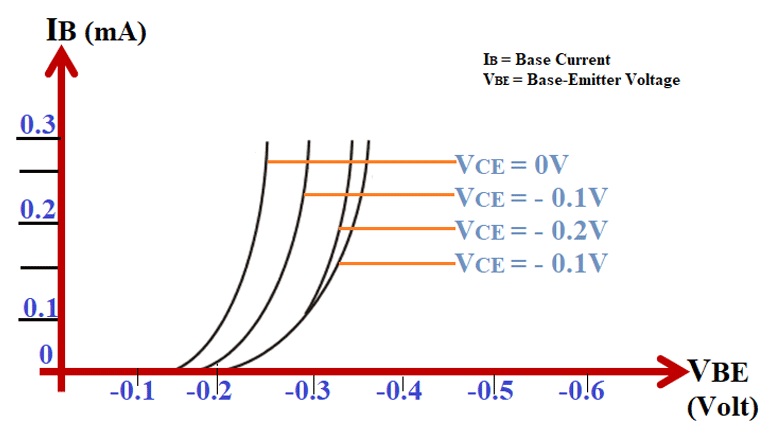
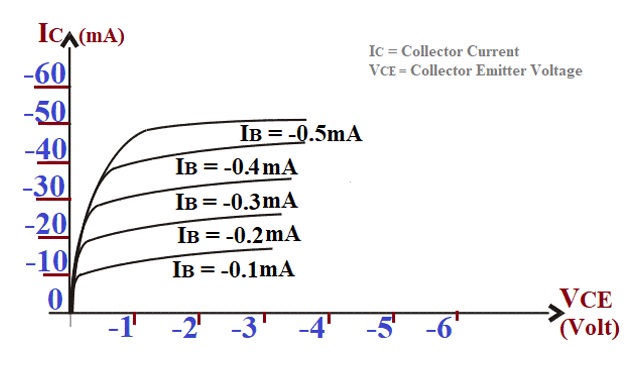
Bipolar Junction Transistors (BJTs) hold the ability to act as both switches and amplifiers, serving as the backbone for a vast array of electronic devices. By applying voltage at the base terminal, a significant current flows through, influencing the opening or closing of the collector-emitter channel. This results in BJTs residing in one of three operational states: active, cutoff, or saturation. Their performance, be it NPN or PNP type, leverages intrinsic semiconductor characteristics, offering adaptability and efficiency in circuitry.
NPN Transistors
In NPN BJTs, the base-emitter junction’s forward bias triggers the movement of electrons from the emitter, passing through a slender, sparsely doped base, into the collector. Predominantly, this electron flow forms the collector current, with minimal recombination losses reflecting an intricate harmony. This movement suggests a carefully orchestrated synergy where the electron supply from the emitter meets the voltage input at the base, showcasing an embodiment of sophisticated engineering practices in contemporary electronics.
PNP Transistors
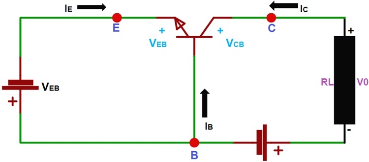
Conversely, PNP transistors utilize holes as their primary charge carriers. Forward-biasing the emitter-base junction permits holes to progress from the emitter into the base, resulting in a collector current directed from the base to the collector. This process is used in circuits demanding the movement of positive charge. Choose between PNPs and NPNs based on specific application needs, demonstrating a profound grasp of material attributes and innovative design principles used to achieve optimal electronic functionality.
Current Interplay and Kirchhoff's Law
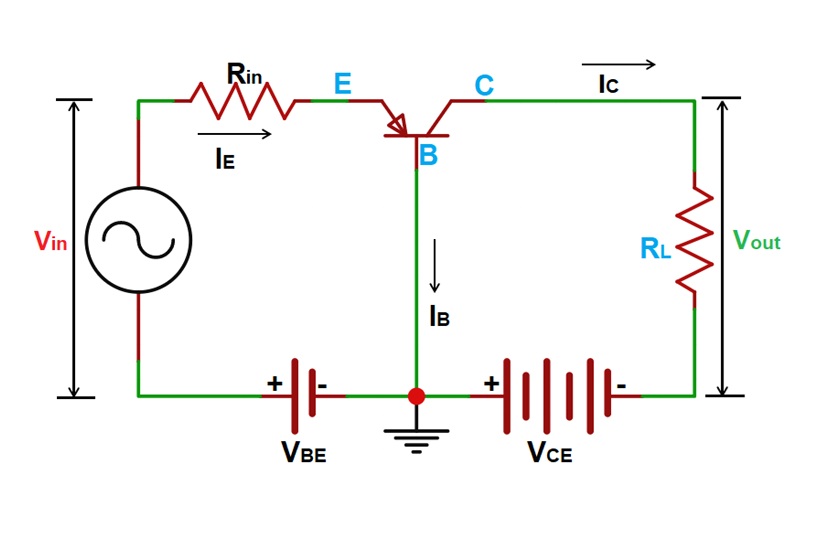
Understanding of BJTs is intricately connected to Kirchhoff’s current law, which articulates that the emitter current (IE) is a composite of the base current (IB) and the collector current (IC), presented as IE = IB + IC. This equation stresses the symbiotic relationship between different currents within transistor circuits, demanding accuracy to preserve circuit performance. In practical settings, prowess in adjusting these relationships is fundamental to enhancing device efficiency and consistency, signifying a melding of theoretical foundations with tangible applications.
BJTs Configuration Types
Bipolar Junction Transistors (BJTs) exhibit a fascinating versatility, adapting to various configurations that each present distinct benefits. The configurations; Common Base, Common Emitter, and Common Collector, differ primarily in their input and output dynamics:
Common Base Configuration
In the domain of electronic circuits, the Common Base configuration is notable for its distinct structural design. The base is grounded, and signals travel through the base-emitter junction to the base-collector junction. Despite exhibiting zero current gain due to its high input impedance, this configuration holds unique traits that suit particular applications.
The Common Base configuration's high input impedance contrasts with its ability to provide stability amid input fluctuations. This quality is especially beneficial in settings where consistent performance is desired despite changes in input conditions. It becomes a go-to option in scenarios where preserving signal integrity under varying influences is paramount.
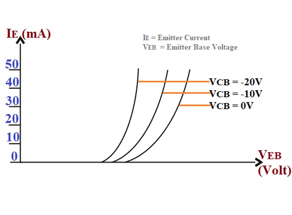
Commonly utilized in RF amplifiers and various high-frequency applications, this configuration is appreciated for its low feedback capacitance. It excels in high-speed operations, where reduced feedback promotes predictable and stable circuit behaviors. Its role is often noted in system designs where precision is required.
Viewing from a broader angle, the absence of current gain adds a layer of strategic value. Although often seen as a limitation, this feature proves useful in cases where signal stability and wider bandwidth are prioritized, while voltage amplification is less critical.
Common Emitter Configuration
The Common Emitter setup distinguishes itself with its capacity for effective signal amplification, utilizing the emitter as a mutual terminal between input and output circuits. This strategic arrangement delivers impressive current and power enhancement, influenced by its contrasting impedance levels, characterized by low input impedance and elevated output impedance, aided by the reverse-biased collector junction.
Successful signal amplification is intertwined with an understanding of impedance behavior. With low input impedance present, there's an increased current flow through the base, amplifying the total current gain significantly. In practical environments, modifying the input signal’s intensity facilitates the optimized transition across the junction, refining the amplification journey.
A notable feature of the Common Emitter arrangement is its power gain, evidenced when output power surpasses input power. This trait proves invaluable in applications demanding substantial signal amplification. This feature is often used by adjusting signal input levels, helping keep amplification stable under different conditions.
Practical use of the Common Emitter calls for a harmonious blend of knowledge and hands-on execution. Daily practice reveals that fine-tuning the input signal and adjusting impedance settings brings tangible improvements to performance.
Contemplating the significance of circuit setups in contemporary electronics, the Common Emitter serves as a conduit between simplicity and operational excellence. Its flexible nature and notable gain potential reflect a design ethos focused on multifunctional applications, indicating the ceaseless evolution of circuit design. This shows a recognition of configurations not merely as technical frameworks but as adaptable solutions to meet the shifting demands of electronic innovation.
Common Collector Configuration
The Common Collector (CC) configuration, widely known as the "emitter follower," serves as a versatile transistor circuit design where the collector serves as the shared connection point. This method is beneficial in situations calling for high input and low output impedance. It acts as an effective medium for facilitating impedance transformation and alignment, thus integrating effortlessly with circuits that demand high input impedance, often reaching hundreds of thousands of ohms.
Among the various benefits of the CC configuration is its role in preserving uniform voltage levels across circuits, making it invaluable in scenarios where maintaining voltage fidelity is of the essence. Its characteristic unity voltage gain makes it perfect for tasks that require signal buffering without increasing the voltage itself. This is commonly utilized in amplifier circuits to produce stable outputs free from distortion. In numerous situations, such as in audio equipment or RF transmission systems, this configuration helps uphold signal integrity when connecting different circuit stages.
Furthermore, the CC configuration is favored in circumstances that necessitate minimal voltage drop, allowing the output voltage to closely mirror the input. This application is considerable in battery-powered devices, where power efficiency is important to prolong operational life. Additionally, its role in impedance bridging is noteworthy; the emitter follower’s low output impedance effectively links high and low impedance stages, reducing signal reflection and attenuation.
The CC configuration is often chosen for its simple operation and reliable ability to keep signals steady. It fits well in circuits that handle different impedance levels, allowing smooth signal matching without complex changes. Effective operation over a wide range of frequencies adds flexibility for many technologies and applications. This balance of simplicity and stable performance supports its continued use in both basic and advanced electronic designs.
BJTs Advantages and Disadvantages
Advantages of BJTs
Bipolar Junction Transistors stand out for their strong high-voltage gain and the ability to switch rapidly. This makes them suitable for scenarios demanding magnification of analog signals and efficient power amplification. The inherent structure of BJTs facilitates the management of large output currents using minimal input currents, proving beneficial in environments where high-gain is desired. They are common in audio and radio frequency amplification, crucially where intricate signal manipulation is necessary.
In various circuit configurations, the low saturation voltage of BJTs enhances energy-efficient performance under specific conditions.
Disadvantages of BJTs
Despite their strengths, BJTs do have limitations. They rely on current control, which demands higher input currents, leading to increased power consumption when compared to field-effect transistors (FETs). Furthermore, BJTs are vulnerable to temperature fluctuations, potentially impacting performance and necessitating comprehensive thermal management. At extreme frequencies, BJTs may experience reduced efficiency, suggesting that other semiconductor devices like FETs may be preferable in such cases.
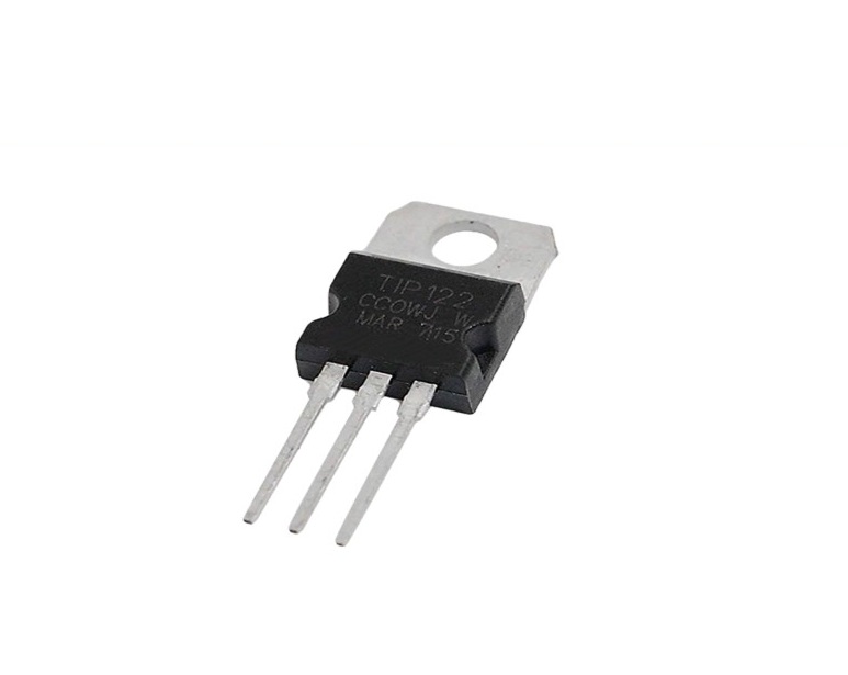
BJT Packaging Options
DDPAK
The DDPAK package is a surface-mount power package designed for BJTs that handle higher current and power levels. It features a large metal tab that helps dissipate heat through the circuit board. This package is commonly used in power regulation and switching applications where efficient thermal performance is required.
SOP (Small Outline Package)
The SOP package is a compact surface-mount format with short leads on both sides. It is suitable for BJTs used in low- to medium-power applications. Its small size allows higher component density, making it common in consumer electronics and signal-level circuits.
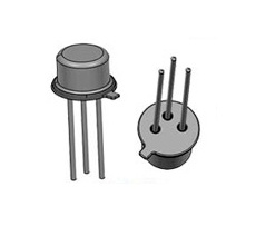
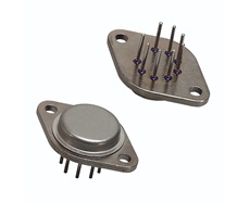
TO-99
The TO-99 package is a metal can package known for its durability and stable electrical performance. It provides good shielding and thermal characteristics, which makes it suitable for precision and low-noise BJT applications. This package is often found in aerospace, instrumentation, and analog signal processing circuits.
QFN (Quad Flat No-Lead)
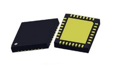
The QFN package is a leadless surface-mount package with contacts underneath the device. It offers low electrical resistance and good thermal conduction through a central pad. BJTs in QFN packages are used in compact, high-performance designs where space and efficiency are important.
TQFP (Thin Quad Flat Package)
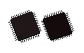
The TQFP package is a flat, square surface-mount package with fine-pitch leads on all four sides. It supports BJTs integrated into complex circuits that require many connections. This package is commonly used in mixed-signal and control applications where compact layout is important.
TO-2205
The TO-2205 package is a variation of the TO-220 family with multiple leads, allowing additional connections or functions. It is designed for BJTs that need moderate to high power handling. The package supports external heatsinks, making it suitable for power amplification and regulation circuits.
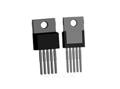
TO-220
The TO-220 package is one of the most widely used through-hole power packages for BJTs. It includes a metal tab that allows direct attachment to a heatsink for effective heat dissipation. This package is commonly used in power amplifiers, motor drivers, and switching regulators.
TO-18
The TO-18 package is a small metal can with good thermal stability and shielding. It is often used for BJTs in low-power and high-frequency applications. Its compact size and reliable construction make it suitable for precision and RF circuits.
TO-3
The TO-3 package is a large metal case designed for high-power BJTs. It provides excellent heat dissipation and mechanical strength. This package is typically used in high-power amplifiers, industrial power supplies, and heavy-duty switching applications.
Conclusion
BJTs remain a reliable choice for signal amplification and switching because they offer strong gain, fast response, and flexible use across many circuit types. By understanding their structure, operating modes, and configurations such as common base, common emitter, and common collector, you can choose the right setup for your circuit goals. At the same time, planning for biasing, power use, and temperature effects helps avoid performance issues and improves stability. With the right design approach and package selection, BJTs continue to support everything from simple amplifiers to demanding power and high frequency applications.
Frequently Asked Questions [FAQ]
1. What is the full form of BJT?
BJT represents a Bipolar Junction Transistor. This fundamental electronic component is integrated into a myriad of circuits. The synergy it brings to complex electronic systems lives in its ability to facilitate intricate signal paths.
2. What is a BJT?
Essentially, a BJT is a semiconductor device with three layers and three terminals, crafting an essential role in the amplification and switching of signals. It stands as a cornerstone in constructing intricate electronic architectures.
3. What are the two primary types of BJTs?
NPN and PNP. These variants exhibit differences in current flow direction and layer structuring, which impacts their practical applications in diverse circuit environments.
4. How does a BJT operate?
The fundamental operation of a BJT involves directing current flow between the emitter and collector, with the base terminal acting as the gatekeeper. This control mechanism is central to the device's function in enhancing signals and facilitating switching actions.
5. In what modes can a BJT function?
BJTs maneuver through three distinct modes; active, cutoff, and saturation. Each mode presents unique functionalities, supporting various roles such as signal amplification and circuit switching.
6. Can you explain transistor gain in a BJT?
Transistor gain is expressed as the relationship between collector current and base current, shedding light on the BJT's capacity to magnify a signal efficiently. This relationship breathes life into the device's ability to enhance electronic communications.
7. How do the common-emitter and common-base configurations contrast?
Exploring configurations reveals that the common-emitter setup boasts high gain and enjoys widespread use for amplification tasks, while the common-base arrangement excels in stability, aligning well with applications reliant on input consistency.
8. Why does biasing matter in BJT circuits?
Biasing tailors the BJT's operating condition, fostering reliability and averting distortion during usage. This adjustment mirrors the careful balance in human emotions, akin to ensuring harmony in electronic symphonies.
9. What is thermal runaway concerning BJTs?
Thermal runaway unfolds when rising temperatures escalate current flow, spiraling into further heating, posing a threat if left unchecked. This phenomenon echoes the delicate equilibrium in human responses to escalating pressures.
10. What benefits do BJTs offer over FETs?
BJTs boast advantages such as elevated voltage gain, robust durability, and resilience to electrostatic discharge, steering them toward high-performance applications demanding reliability and enduring strength.
11. Are there any constraints associated with BJTs?
While BJTs excel in many areas, challenges arise as they consume more power, are prone to temperature fluctuations, and present lower input impedance than FETs, which may restrict their appeal in certain circuit designs.
Related Blog
-
How Many Zeros in a Million, Billion, Trillion?
![How Many Zeros in a Million, Billion, Trillion?]()
July 29th, 2024
Million represents 106, an easily graspable figure when compared to everyday items or annual salaries. Billion, equivalent to 109, starts to stretch t... -
IRLZ44N MOSFET Datasheet, Circuit, Equivalent, Pinout
![IRLZ44N MOSFET Datasheet, Circuit, Equivalent, Pinout]()
August 28th, 2024
The IRLZ44N is a widely-used N-Channel Power MOSFET. Renowned for its excellent switching capabilities, it is highly suited for numerous applications,... -
Battery Temperature Too Low, Charging Stopped. How to Fix It?
![Battery Temperature Too Low, Charging Stopped. How to Fix It?]()
October 6th, 2024
Mobile phone battery charging issues are common but can be effectively managed. Temperature plays a big role in battery efficiency, as smartphone batt... -
BC547 Transistor Comprehensive Guide
![BC547 Transistor Comprehensive Guide]()
July 4th, 2024
The BC547 transistor is commonly used in a variety of electronic applications, ranging from basic signal amplifiers to complex oscillator circuits and... -
Comprehensive Guide to SCR (Silicon Controlled Rectifier)
![Comprehensive Guide to SCR (Silicon Controlled Rectifier)]()
April 22th, 2024
Silicon Controlled Rectifiers (SCR), or thyristors, play a pivotal role in power electronics technology because of their performance and reliability. ... -
LR621, SR621SW, 364, AG1 Battery Equivalents and Replacements
![LR621, SR621SW, 364, AG1 Battery Equivalents and Replacements]()
July 15th, 2024
LR621 and SR621SW button batteries are prevalent in compact electronic devices like watches, small toys, calculators, and remote keys. Multiple manufa... -
Fundamentals of Op-Amp Circuits
![Fundamentals of Op-Amp Circuits]()
December 28th, 2023
In the intricate world of electronics, a journey into its mysteries invariably leads us to a kaleidoscope of circuit components, both exquisite and co... -
Comparing NMOS and PMOS Differences and Applications
![Comparing NMOS and PMOS Differences and Applications]()
November 15th, 2024
Understanding the differences between NMOS and PMOS transistors is important in designing efficient circuits. NMOS (N-type Metal-Oxide-Semiconductor) ... -
A Complete Guide to Multiplexers and Their Role in Digital Systems
![A Complete Guide to Multiplexers and Their Role in Digital Systems]()
September 20th, 2025
Multiplexers are components in digital systems, designed to channel multiple input signals into a single output line using binary logic and control si... -
What Do STD, AGM, and Gel Mean On a Battery Charger
![What Do STD, AGM, and Gel Mean On a Battery Charger]()
July 10th, 2024
Traditional lead-acid battery chargers are known for their simplicity and reliability. They have been serving their purpose effectively for years, lar...


Hot Parts
- AD53098
- SC32442B54-7080
- C2012C0G2E682J125AA
- EN87C196KD20
- CGA7K1X7R3D102K130KA
- TMP87C405AM-3UP4
- MC74VHC540DTR2G
- CY25812SXC
- SP331ET-L/TR
- TPS65011RGZ
- EP2C20F484I8
- X9317UV8ZT1
- OPA4134UA/2.5K
- T494A106M016AH
- PBL38621/2R3
- SC6620-200G
- PNX1502E/G
- PIC16C54C-04/P
- RT1206BRE07220KL
- MCP6032T-E/MS
- 08055A220JAT2A
- ZL30120GGG2
- MM908E622ACDWB
- MN101C01DAH
- W25Q32FVTCIG
- C1608X8R1H333M080AE
- NCV33064D-5R2
- CL10B392KB8NNND
- SC540219FCR2
- FT150R12KE3G_B4
- GRM319R71C105KAA3J
- C1005X8R1H471M050BA
- OPA4227UA
- DS3695AMX/NOPB
- 08055A681JAQ2A
- GQM1555C2D1R4CB01D
- ADM696ARZ-REEL
- 30EPH06
- GS7966-424-006BB
- GRM1555C1E5R4CZ01D
- T409H336K015BC4251
- CKF-38-78010
- 74LVX14DT
- CY22392ZC-335
- CY7C429-15VC
- SSCE5V011N7
- MAX6029EUK41
- ATF1508AS-20QC100
- 6ES7322-1BH01-0AA0
- R2A30434BG