- English
-
EnglishDeutschItaliaFrançais한국의русскийSvenskaNederlandespañolPortuguêspolski繁体中文SuomiGaeilgeSlovenskáSlovenijaČeštinaMelayuMagyarországHrvatskaDanskromânescIndonesiaΕλλάδαБългарски езикGalegolietuviųMaoriRepublika e ShqipërisëالعربيةአማርኛAzərbaycanEesti VabariikEuskeraБеларусьLëtzebuergeschAyitiAfrikaansBosnaíslenskaCambodiaမြန်မာМонголулсМакедонскиmalaɡasʲພາສາລາວKurdîსაქართველოIsiXhosaفارسیisiZuluPilipinoසිංහලTürk diliTiếng ViệtहिंदीТоҷикӣاردوภาษาไทยO'zbekKongeriketবাংলা ভাষারChicheŵaSamoa日本語SesothoCрпскиKiswahiliУкраїнаनेपालीעִבְרִיתپښتوКыргыз тилиҚазақшаCatalàCorsaLatviešuHausaગુજરાતીಕನ್ನಡkannaḍaमराठी
A Beginner's Guide to IC Packages, Types, and Selections
Catalog
IC Fabrication
The fabrication of Integrated Circuits (IC) is a fascinating journey, turning raw, inanimate materials into vibrant electronic circuits through meticulous processes. To truly grasp its details, one should explore every facet, appreciating the harmony among various techniques and the evolutionary path innovations have carved in this dynamic field.
Lithography
Lithography serves as the gateway to IC production. Beginning with a photoresist layer laid delicately onto a silicon wafer, this process demands a perfect blend of chemical finesse and precision. The intriguing step of solidifying this layer involves baking, ensuring its readiness for the subsequent light exposure through a reticle, which functions like an intricate stencil, exposing desired patterns. The elegance of lithography lies in the precise dance of light and patterns, each choice a whisper to the future stages of creation.
Etching and Deposition
With patterns in place, etching unfolds its dual nature, employing both dry and wet methods to carefully strip away unwelcome material, exposing the circuit's heart. Deposition, the art of addition, is akin to sculpting where material layers are painstakingly built up. Through advanced techniques like chemical vapor deposition, these layers are crafted to form components and barriers, ideal to an IC’s destined role. Each deft touch serves the circuit's intricate purpose.
Chemical Mechanical Polishing
Chemical mechanical polishing (CMP) is where chemistry waltzes with mechanics, achieving surfaces of unparalleled smoothness. The challenge dances in maintaining surface uniformity while eschewing defects. The slurry used is a balanced elixir of abrasion and chemical action, offering a detailed polish that is both gentle and comprehensive.
Oxidation
Oxidation wields the power to transform the wafer's state, turning silicon to silicon dioxide. With both dry and wet methods in play, it fine-tunes the wafer’s thermal and electrical demeanor, setting the stage for IC resilience. To master this phase, one must delve into the intimate dance between heat, silicon, and oxygen, their reactions echo across the wafer's surface, rich and vivid.
Ion Implantation and Diffusion
Ion implantation steps forward, propelling ionized particles to embed impurities with exactitude. Following this, diffusion sweeps in, healing implantation scars and forging uniform doping profiles. Both methods illustrate a delicate equilibrium, implantation demands calculated ion distribution, while diffusion thrives under controlled heat conditions, perfecting the lattice form with subtle artistry.
IC fabrication tells a tale of relentless creativity and daring experimentation. Lessons woven from experience underline the profound impact of minor tweaks across phases, enhancing performance and efficiency. Evolving techniques showcase the need for flexibility and vision, key to embracing new innovations. Thus, the craft of IC manufacturing marches ahead, always at the cutting edge of technological wonder.
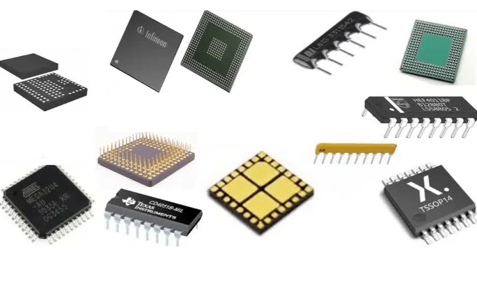
IC Packaging Types
Integrated circuit (IC) packaging comes in various forms, primarily determined by mounting methods: through-hole and surface mount solutions. Each possesses its unique characteristics and specific uses, reflecting our diverse needs in the electronics landscape.
Through-Hole Packages
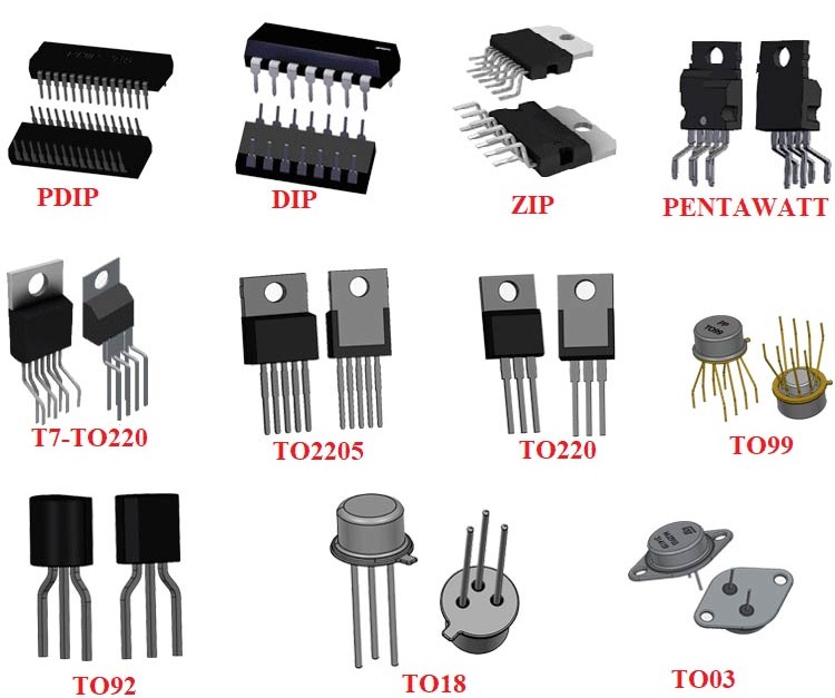
This classic packaging style features pins that penetrate circuit board holes for a soldered connection. Although it requires more space, this approach offers resilience and the convenience of manual assembly, often found appealing in prototyping and educational settings. Dual Inline Packages (DIP) are notable here, frequently made from ceramic or plastic, and remain favored for their adaptability in developmental applications with lower frequencies. For instance, the 28-pin ATmega328 microcontroller fits effortlessly into breadboards, minimizing the chances of electrical shorts. Variants like Plastic Dual In-Line (PDIP) and Molded Dual In-Line (MDIP) distinguish themselves by pin spacing standard, skinny, and shrink. Additionally, Zig-Zag Inline Packages (ZIP), ceramic-encased CER-DIPs, and Pin Grid Arrays (PGA) offer distinct advantages for diverse hardware implementations.
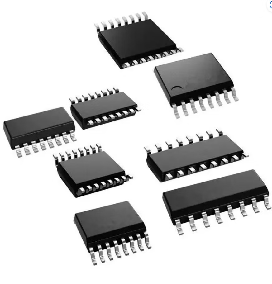
Surface Mount Packages
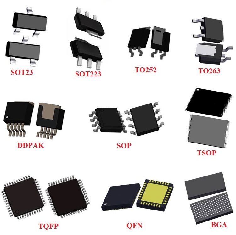
In contrast, surface mount technology (SMT) applies components directly onto the printed circuit board (PCB), elevating both manufacturing efficiency and electrical functionality. SMT packages, crafted from plastic or ceramic, conserve space, enabling the creation of intricate, compact electronic designs. Within this field, various package types are instrumental:
• Small Outline L-leaded packages, suited for streamlined profile applications.
• Quad Flat L-leaded Packages (QFP), which effectively manage heat with ample contact points.
• Ball Grid Arrays (BGA), maximizing board space with solder ball connectivity.
Moreover, Fine Pitch Land Grid Arrays support high-density interconnections, while Wafer Level Chip Size Packages align component dimensions with the silicon wafer, creating minimal footprint designs.
Each packaging strategy reveals specific advantages. Surface mount technology supports denser placements and improved electromagnetic compatibility, aligning with advanced automated production methods that help manage expenses. These attributes, however, contrast with the straightforward assembly of through-hole packages, making them well-suited for breadboard experimentation and situations demanding durable physical encasement. Engaging with SMT components in experimental projects often calls for creativity, such as deploying custom PCBs or carriers. Though they serve different purposes, both packaging types are used in the evolution of electronic technology, showing the intricate balance between innovation, functionality, and thoughtful design adapting to our technological desires.
Choosing the Best IC Package for Specific Needs
Packaging serves to protect integrated circuits (ICs), preventing potential damage while supporting assembly and aiding in thermal management. Making a choice for IC packages involves a detailed assessment of various elements, each shaping the package's appropriateness for different applications.
Several factors come into play when selecting an IC package. Convenience in assembly facilitates smooth incorporation into the current system, involving a detailed look at the assembly method to prevent issues and streamline production. Power demands have a significant impact on the package's capacity to accommodate different power levels, ensuring the IC's optimal function and durability.
Finding a balance between affordability and performance is a central theme in IC package selection. Budget-aware projects need to align costs with performance expectations. It makes sense to evaluate the overall cost of ownership, taking into account initial expenses alongside long-term reliability and upkeep costs. Achieving this balance frequently relies on thorough market research to seize the most economical yet effective options available.
Connectivity greatly influences the IC's communication proficiency with other components, making its evaluation necessary for system compatibility. As technology swiftly progresses, emerging packaging solutions offer enhanced functionalities and performance upgrades. Keeping up with these changes aids in informed decision-making, exploiting state-of-the-art innovations to fulfill system requisites.
The right IC package selection can affect system efficiency and trustworthiness. Practical applications have shown that emphasizing heat dissipation capabilities can greatly improve performance, especially in demanding power situations. These observations, collected from a diverse range of projects, emphasize aligning package features with distinct operational aims to achieve successful results.
Conclusion
From wafer processing to final packaging, every step in IC production influences cost, performance, and reliability. Fabrication techniques ensure miniaturization and precision, while package selection balances space, power, and assembly needs. Choosing the right combination supports long-term functionality and efficient design, helps meet specific technical and market requirements in today’s fast-evolving electronics landscape.
Related Blog
-
How Many Zeros in a Million, Billion, Trillion?
![How Many Zeros in a Million, Billion, Trillion?]()
July 29th, 2024
Million represents 106, an easily graspable figure when compared to everyday items or annual salaries. Billion, equivalent to 109, starts to stretch t... -
IRLZ44N MOSFET Datasheet, Circuit, Equivalent, Pinout
![IRLZ44N MOSFET Datasheet, Circuit, Equivalent, Pinout]()
August 28th, 2024
The IRLZ44N is a widely-used N-Channel Power MOSFET. Renowned for its excellent switching capabilities, it is highly suited for numerous applications,... -
Battery Temperature Too Low, Charging Stopped. How to Fix It?
![Battery Temperature Too Low, Charging Stopped. How to Fix It?]()
October 6th, 2024
Mobile phone battery charging issues are common but can be effectively managed. Temperature plays a big role in battery efficiency, as smartphone batt... -
BC547 Transistor Comprehensive Guide
![BC547 Transistor Comprehensive Guide]()
July 4th, 2024
The BC547 transistor is commonly used in a variety of electronic applications, ranging from basic signal amplifiers to complex oscillator circuits and... -
Comprehensive Guide to SCR (Silicon Controlled Rectifier)
![Comprehensive Guide to SCR (Silicon Controlled Rectifier)]()
April 22th, 2024
Silicon Controlled Rectifiers (SCR), or thyristors, play a pivotal role in power electronics technology because of their performance and reliability. ... -
LR621, SR621SW, 364, AG1 Battery Equivalents and Replacements
![LR621, SR621SW, 364, AG1 Battery Equivalents and Replacements]()
July 15th, 2024
LR621 and SR621SW button batteries are prevalent in compact electronic devices like watches, small toys, calculators, and remote keys. Multiple manufa... -
Fundamentals of Op-Amp Circuits
![Fundamentals of Op-Amp Circuits]()
December 28th, 2023
In the intricate world of electronics, a journey into its mysteries invariably leads us to a kaleidoscope of circuit components, both exquisite and co... -
Comparing NMOS and PMOS Differences and Applications
![Comparing NMOS and PMOS Differences and Applications]()
November 15th, 2024
Understanding the differences between NMOS and PMOS transistors is important in designing efficient circuits. NMOS (N-type Metal-Oxide-Semiconductor) ... -
A Complete Guide to Multiplexers and Their Role in Digital Systems
![A Complete Guide to Multiplexers and Their Role in Digital Systems]()
September 20th, 2025
Multiplexers are components in digital systems, designed to channel multiple input signals into a single output line using binary logic and control si... -
What Do STD, AGM, and Gel Mean On a Battery Charger
![What Do STD, AGM, and Gel Mean On a Battery Charger]()
July 10th, 2024
Traditional lead-acid battery chargers are known for their simplicity and reliability. They have been serving their purpose effectively for years, lar...


Hot Parts
- EP3SL200F1152C4N
- DS89C21TM/NOPB
- LTC4282IUH#PBF
- TMA1215D
- LC72323Y-9304N-E
- MP2361DK
- BCM56322A0KFEBG
- FST3257QSC
- SI2493-C-FT
- EL4543IU
- SN65HVD82D
- LM21212MH-2/NOPB
- CSC4863FN
- TMP90C441FG
- CL21B475KOQVPJE
- CGA3E2C0G1H030C080AA
- DAC7800KU/1K
- MPX2200GP
- 12063A822JAT2A
- MIC803-26D3VC3-TR
- PIC18F45K22-I/P
- MAX3232EIPWR
- TLE7189FXUMA2
- CC0805JRNPO9BN271
- 06035C561KAT9A
- PEX8749-CA80BCG
- AN32053AAPR
- HMC734LP5ETR
- PIC18LF14K22-I/SO
- ISO7420FCCD
- TPS3808G33DBVT
- QMK212B7102MD-T
- SKM195GB128D
- MICRF211AYQS
- C1005JB1E474M050BB
- GRM1555C2A5R9DA01J
- 0805YA681KAT2A
- TPSD156K025H0100
- ATMEGA48-20AJ
- VI-JWJ-EY
- HC1S80F1020NAM
- T491D476K016AT4802
- CWR09KC106KBB
- VE-2W0-EW
- M29F040-70K1
- EN39SL160AL-70NIP
- T73LC03AIV
- OPA832AIDR
- SPCA504B
- TC9327AF-639