- English
-
EnglishDeutschItaliaFrançais한국의русскийSvenskaNederlandespañolPortuguêspolski繁体中文SuomiGaeilgeSlovenskáSlovenijaČeštinaMelayuMagyarországHrvatskaDanskromânescIndonesiaΕλλάδαБългарски езикGalegolietuviųMaoriRepublika e ShqipërisëالعربيةአማርኛAzərbaycanEesti VabariikEuskeraБеларусьLëtzebuergeschAyitiAfrikaansBosnaíslenskaCambodiaမြန်မာМонголулсМакедонскиmalaɡasʲພາສາລາວKurdîსაქართველოIsiXhosaفارسیisiZuluPilipinoසිංහලTürk diliTiếng ViệtहिंदीТоҷикӣاردوภาษาไทยO'zbekKongeriketবাংলা ভাষারChicheŵaSamoa日本語SesothoCрпскиKiswahiliУкраїнаनेपालीעִבְרִיתپښتوКыргыз тилиҚазақшаCatalàCorsaLatviešuHausaગુજરાતીಕನ್ನಡkannaḍaमराठी
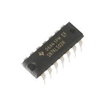
74LS02 Quad 2-Input NOR Gate IC: Pinout, Working, Dimensions and Applications
Catalog
Overview to the 74LS02 Integrated Circuit
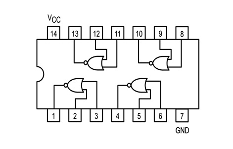
The 74LS02 integrated circuit features four independent 2-input NOR gates, forming the bedrock of many TTL-based digital logic systems. Each NOR gate's high output manifests solely when both inputs are low; otherwise, a high input enforces a low output. This circuit thrives on Low-Power Schottky Transistor-Transistor Logic (TTL) technology, efficiently applying a 5V supply to enhance power use while maintaining reliable performance. It finds significant applications in systems such as logic control circuits, elementary memory units, decoding arrangements, and within combinational logic frameworks. This multifaceted component finds its niche in scenarios frequently calling for dependable NOR gate function.
The 74LS02 transcends basic switching tasks, ideal in developing complex logic structures. Within control systems, it enhances decision-making by facilitating operations conditional on multiple signal states. Hands-on experiences reveal that these ICs offer a path to seamless adjustments in logical systems, sharpening operational efficiency without requiring extensive system redesign.
In the domain of logic design, the utility of the 74LS02 is manifest through the development of intricate architectures. It is integral to creating essential logic configurations like SR latches and multiplexers. Through dedicated development practices, its influence is apparent in progressing digital designs, offering a robust foundation for complex circuits without involving advanced components, thus minimizing complexity and potential points of failure.
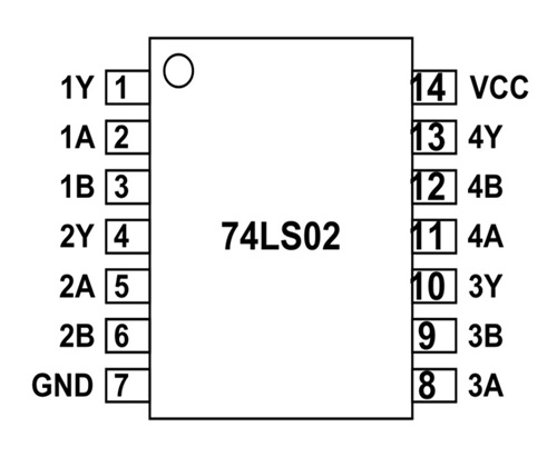
74LS02 Pin Configuration Insights
|
Pin Number |
Description |
|
NORGATE 1 |
|
|
2 |
1A-INPUT1 of GATE 1 |
|
3 |
1B-INPUT2 of GATE 1 |
|
1 |
1Y-OUTPUT of GATE1 |
|
NORGATE 2 |
|
|
5 |
2A-INPUT1 of GATE 2 |
|
6 |
2B-INPUT2 of GATE 2 |
|
4 |
2Y-OUTPUT of GATE2 |
|
NORGATE 3 |
|
|
8 |
3A-INPUT1 of GATE 3 |
|
9 |
3B-INPUT2 of GATE 3 |
|
10 |
3Y-OUTPUT of GATE3 |
|
NORGATE 4 |
|
|
11 |
4A-INPUT1 of GATE 4 |
|
12 |
4B-INPUT2 of GATE 4 |
|
13 |
4Y-OUTPUT of GATE4 |
|
SHARED TERMINALS |
|
|
7 |
GND- Connected to ground |
|
14 |
VCC-Connected to positive voltage to provide power to all
four gates |
74LS02 Technical Specifications
|
Parameter |
Specification |
|
Operating Voltage Range |
+4.75 V to +5.25 V |
|
Maximum Supply Voltage |
7 V |
|
Maximum Output Current per Gate |
8 mA |
|
Output Type |
TTL Outputs |
|
Power Consumption |
Low Power |
|
Maximum ESD Protection |
3.5 kV |
|
Typical Rise Time |
15 ns |
|
Typical Fall Time |
15 ns |
|
Operating Temperature Range |
0°C to 70°C |
|
Storage Temperature Range |
-65°C to 150°C |
74LS02 Substitute Options
IC 7402
Applications of the 74LS02
NOR-Based Logic Designs
The 74LS02 contains four independent 2-input NOR gates in one package, making it a practical choice for circuits built around NOR logic. Since a NOR gate is a universal gate, it can also be configured to perform other logic functions such as NOT, OR, and even more complex combinations. This allows building flexible control paths using fewer components while keeping the circuit layout simple and organized.
High-Speed Switching and Efficient Design
Built with Schottky TTL technology, the 74LS02 supports fast switching, which makes it suitable for timing paths, signal processing, and combinational logic where quick response matters. At the same time, LS-TTL design reduces power consumption compared to older TTL families. This balance of speed and efficiency makes it a reliable option for practical, cost-conscious digital systems.
TTL Compatibility and System Integration
The 74LS02 is designed to operate with standard 5 V TTL levels, allowing it to connect smoothly with other TTL components. This reduces compatibility issues when integrating it into larger digital systems. Because of its stable and predictable behavior, it remains widely used in both educational circuits and long-standing industrial designs.
Practical Use Across Digital Systems
The 74LS02 plays a steady role in many digital applications. It is used in general logic functions for combining and inverting signals. In digital electronics, it supports control logic and decision-making paths. Within arithmetic logic units, it helps implement comparison and control operations. It also appears in memory and data-handling circuits where reliable logic processing is required.
In networking and communication systems, the 74LS02 assists with signal conditioning and control logic to maintain stable data flow. Its broad use across computing, control, and communication hardware shows its lasting value. Even as technology advances, the 74LS02 continues to serve as a dependable building block in digital design.
Operations of NOR Gate
Inside each NOR gate of the 74LS02, the essential OR and NOT operations come together harmoniously. The equation NOR = OR + NOT elegantly captures this dual capability, enabling versatile approaches to fundamental logic tasks. The structural arrangement of components in this configuration emphasizes the clear and practical nature of digital logic.
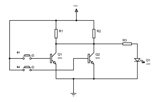
In practical settings, NOR operations are configured using two transistors, which allow for input manipulation through simple button presses. This hands-on experience engages directly with the circuit, revealing LED indicator responses that depict different output conditions. For instance, when both inputs are low, the LED shines brightly; if one input is high, the LED goes dark; maintaining darkness when both inputs are high. These scenarios foster direct interaction and an intuitive grasp of digital circuit principles through experimentation.
Engagement with the 74LS02 offers encounters with three logic states, which can be vividly demonstrated through output indications. A high output occurs when both inputs are low, an event that can be used in designing circuits with specific activation criteria. In contrast, a low output arises when either or both inputs are high, acting as a safeguard against unwanted operations. This practical demonstration of the expression Y = A + B facilitates deeper understanding and supports constructing sophisticated logical architectures that underpin many computing systems.
The seemingly modest abilities of the NOR gate mask its profound potential for executing fundamental logic tasks. Serving as foundational elements for more intricate circuits, especially in resource-limited scenarios, NOR gates furnish inventive solutions across diverse technological fields. By recognizing the value in simplicity, the 74LS02 inspires efficient yet fully functional circuit designs, merging historical insights with modern applications for optimal outcomes.
74LS02 Dimensions
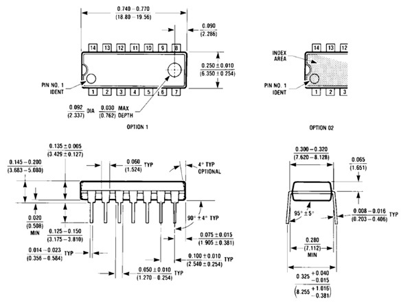
The packaging dimension drawing of the 74LS02 shows the physical structure of the 14-pin Dual In-Line Package used for through-hole mounting. The top view outlines the rectangular body and clearly marks the pin numbering from 1 to 14. A notch and index area indicate the orientation of the IC, helping you correctly identify Pin 1 before installation. The overall body length and width are labeled with minimum and maximum values, allowing accurate PCB layout planning.
The side view explains the vertical profile of the package. It shows the body height above the seating plane and the length of the leads that extend downward into the board. The seating plane acts as the reference surface when the IC is mounted on a PCB. This helps determine clearance and soldering alignment.
The front view focuses on the lead spacing and bend angles. It shows the standard 0.1-inch pin pitch between adjacent leads, which matches common DIP socket and PCB footprints. The drawing also specifies lead width, thickness, and allowable tolerances to ensure reliable insertion into plated through-holes.
Conclusion
Overall, the 74LS02 remains a dependable choice for digital designs that need stable NOR logic, quick response time, and easy integration with other TTL-level components. Its four-gate layout supports flexible logic design, from basic signal combining and inversion to building blocks like SR latches, multiplexing logic, and control or decision paths in computing and communication hardware. If a substitute is needed, parts like SN54LS02, 7402, or HCF4077 may be considered depending on environment and technology family, but the 74LS02 continues to be a practical, widely used NOR gate IC.
Related Blog
-
How Many Zeros in a Million, Billion, Trillion?
![How Many Zeros in a Million, Billion, Trillion?]()
July 29th, 2024
Million represents 106, an easily graspable figure when compared to everyday items or annual salaries. Billion, equivalent to 109, starts to stretch t... -
IRLZ44N MOSFET Datasheet, Circuit, Equivalent, Pinout
![IRLZ44N MOSFET Datasheet, Circuit, Equivalent, Pinout]()
August 28th, 2024
The IRLZ44N is a widely-used N-Channel Power MOSFET. Renowned for its excellent switching capabilities, it is highly suited for numerous applications,... -
Battery Temperature Too Low, Charging Stopped. How to Fix It?
![Battery Temperature Too Low, Charging Stopped. How to Fix It?]()
October 6th, 2024
Mobile phone battery charging issues are common but can be effectively managed. Temperature plays a big role in battery efficiency, as smartphone batt... -
BC547 Transistor Comprehensive Guide
![BC547 Transistor Comprehensive Guide]()
July 4th, 2024
The BC547 transistor is commonly used in a variety of electronic applications, ranging from basic signal amplifiers to complex oscillator circuits and... -
Comprehensive Guide to SCR (Silicon Controlled Rectifier)
![Comprehensive Guide to SCR (Silicon Controlled Rectifier)]()
April 22th, 2024
Silicon Controlled Rectifiers (SCR), or thyristors, play a pivotal role in power electronics technology because of their performance and reliability. ... -
LR621, SR621SW, 364, AG1 Battery Equivalents and Replacements
![LR621, SR621SW, 364, AG1 Battery Equivalents and Replacements]()
July 15th, 2024
LR621 and SR621SW button batteries are prevalent in compact electronic devices like watches, small toys, calculators, and remote keys. Multiple manufa... -
Fundamentals of Op-Amp Circuits
![Fundamentals of Op-Amp Circuits]()
December 28th, 2023
In the intricate world of electronics, a journey into its mysteries invariably leads us to a kaleidoscope of circuit components, both exquisite and co... -
Comparing NMOS and PMOS Differences and Applications
![Comparing NMOS and PMOS Differences and Applications]()
November 15th, 2024
Understanding the differences between NMOS and PMOS transistors is important in designing efficient circuits. NMOS (N-type Metal-Oxide-Semiconductor) ... -
A Complete Guide to Multiplexers and Their Role in Digital Systems
![A Complete Guide to Multiplexers and Their Role in Digital Systems]()
September 20th, 2025
Multiplexers are components in digital systems, designed to channel multiple input signals into a single output line using binary logic and control si... -
What Do STD, AGM, and Gel Mean On a Battery Charger
![What Do STD, AGM, and Gel Mean On a Battery Charger]()
July 10th, 2024
Traditional lead-acid battery chargers are known for their simplicity and reliability. They have been serving their purpose effectively for years, lar...


Hot Parts
- GCM1885C2A5R9DA16D
- LM4843MHX
- CBS3504824
- TAP226K020SRS
- AD7879-1ACPZ-500R7
- SI7842DP-T1-GE3
- JS28F320J3D75B
- ACM4520-901-2P-TL000
- KH29LV320DBTC-70G
- DAC716UK
- MC74LS161A
- AT28C64-25SI
- ADM809SARTZ-REEL
- LE25FS406LF
- LM3880MFE-1AD
- CY2309ZXI-1H
- MAX3013EUP+
- CXM3006R-T4
- LBZT52C3V6T1G
- THS4081IDGNR
- C1005NP01H220J050BA
- GRM0336T1E6R2DD01D
- SN65LVDS2DBVT
- LM50CIM3/NOPB
- CWR11JB335KB
- SST39SF010-70-4C-NH
- BT812KPF
- CA91L862A-50IL
- TAJB335M020RNJ
- 2220HA391JAT1A
- 24AA256-I/SN
- CY29972AXI
- SSD2543QT6A
- XC5VTX150T-1FFG1156C
- DVC5402GGU100
- C8051F123
- ST72F324J2T6
- LT1112CS8
- TMA463-48LQI
- JTC0624S15
- T491B226M010ZT7290
- LTM4628EV#PBF
- T491A335K006AT4838
- LTC1472SL
- XC2S200E-4PQG208I
- SLF12575T-330M3R2-
- MJW15-12S15
- TCAN4550RGYR
- M30622MHP-E53GP
- C1608X7R1C224K