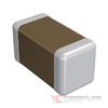
Product overview – Murata GRM1555C1H1R8CZ01J
Murata Electronics GRM1555C1H1R8CZ01J is a multilayer ceramic chip capacitor designed for applications that require tight capacitance tolerance and stable behavior over temperature, frequency, and time. It is part of Murata’s GRM series and uses a C0G/NP0 dielectric, which is known for low loss and minimal capacitance variation in demanding analog and RF environments.
Key basic parameters of the GRM1555C1H1R8CZ01J include:
- Capacitance: 1.8 pF
- Tolerance: ±0.25 pF
- Rated voltage: 50 V
- Dielectric: C0G / NP0
- Package size: 0402 (1005 metric)
These parameters make GRM1555C1H1R8CZ01J suitable where small capacitance values with predictable, repeatable behavior are required, such as RF matching networks, high‑frequency filters, precision timing and measurement circuits, and low‑drift analog signal paths.
Core electrical characteristics of GRM1555C1H1R8CZ01J
At the core of GRM1555C1H1R8CZ01J is a 1.8 pF nominal capacitance with a tight ±0.25 pF tolerance. In practice, this means the part will remain within a relatively narrow capacitance window across units, which is beneficial when designing narrowband filters, impedance‑matching sections, or tuned circuits where a small change in capacitance can shift resonance frequency noticeably.
The 50 V rating of GRM1555C1H1R8CZ01J provides headroom for many low‑ to medium‑voltage signal chains and RF stages. In resonant and RF environments, designers often derate capacitors for reliability and to control non‑ideal behavior. A 50 V rating for a 1.8 pF element in 0402 format allows comfortable use in typical 3.3 V, 5 V, 12 V, and many RF front‑end conditions, as long as the actual RF voltages at the capacitor terminals remain within the specified limits over the full operating range.
The C0G/NP0 dielectric used in GRM1555C1H1R8CZ01J is a key differentiator compared with higher‑K dielectrics (such as X7R or Y5V). C0G/NP0 provides:
- Low dielectric loss, supporting high‑Q and low‑ESR behavior at RF
- Minimal capacitance variation over temperature
- Negligible voltage dependence compared with class II dielectrics
- Predictable long‑term stability (low aging)
In a practical RF band‑pass filter example at hundreds of MHz, replacing a C0G/NP0 part such as GRM1555C1H1R8CZ01J with a higher‑K dielectric device of similar nominal value can result in noticeable drift of center frequency and insertion loss over temperature and applied voltage. Using the C0G/NP0 dielectric keeps the response closer to the design intent across operating conditions.
Temperature and aging behavior of GRM1555C1H1R8CZ01J
GRM1555C1H1R8CZ01J follows the C0G/NP0 temperature characteristic, which is typically specified as a near‑flat capacitance curve over a defined temperature range. C0G/NP0 dielectrics are characterized by:
- Capacitance change vs. temperature that is close to zero, often within a small fraction of a percent over the operating range.
- Absence of phase transitions that cause abrupt capacitance shifts in some higher‑K ceramics.
For GRM1555C1H1R8CZ01J, this behavior allows temperature‑stable timing, filtering and impedance functions. In a typical temperature sweep from sub‑zero ambient up to elevated operating temperatures, the capacitance remains close to its nominal value plus tolerance, helping filter corner frequencies, resonant points and phase characteristics remain stable.
The GRM series data for GRM1555C1H1R8CZ01J also includes “Capacitance Change – Aging.” C0G/NP0 capacitors exhibit negligible capacitive aging compared with class II dielectrics. In practice, this means that the capacitance value of GRM1555C1H1R8CZ01J will remain effectively constant over years of operation, rather than decreasing with log‑time. For long‑life equipment (infrastructure, industrial control, test and measurement), low aging minimizes the need to over‑design or compensate for gradual capacitance drift.
Frequency‑dependent performance of GRM1555C1H1R8CZ01J
GRM1555C1H1R8CZ01J is characterized in the GRM series documentation for several frequency‑related parameters:
- Impedance – Frequency Characteristics:
As frequency increases, the impedance of a capacitor decreases until reaching its self‑resonant frequency (SRF), where parasitic inductance and capacitance balance. Above SRF, the device begins to behave inductively. GRM1555C1H1R8CZ01J, with its small 1.8 pF value and 0402 geometry, typically exhibits an SRF in the high‑MHz to GHz range, depending on layout and surrounding circuitry. This makes it suitable for RF matching, coupling, and decoupling applications where operation near or below SRF is desired.
- Allowable Apparent Power – Frequency:
As frequency rises, dielectric and conduction losses in the capacitor lead to heating. The GRM series data for GRM1555C1H1R8CZ01J specifies how much apparent power can be applied at different frequencies without exceeding thermal limits. In a high‑frequency power amplifier output matching network, for example, this parameter helps determine whether the capacitor can handle RF power levels without excessive temperature rise.
- Allowable Voltage – Frequency:
The permissible applied voltage may be frequency‑dependent due to loss and heating. At higher frequencies, GRM1555C1H1R8CZ01J may need to be operated at voltages lower than the DC rating to maintain reliability. This is relevant in resonant circuits where RF voltages across small capacitors can substantially exceed the source voltage.
- Allowable Current – Frequency:
Current through a capacitor increases with frequency for a given voltage amplitude. The GRM series characterization of GRM1555C1H1R8CZ01J provides limits for this current over frequency so that conduction and dielectric losses remain within safe bounds. In RF decoupling or high‑Q resonant circuits, checking allowable current vs. frequency helps avoid overheating the part due to reactive current.
A concrete example: in a 900 MHz matching network, the designer can use the impedance‑frequency curve of GRM1555C1H1R8CZ01J to select an operating point comfortably below the self‑resonant frequency and then apply the allowable current and apparent power curves to confirm that RF voltage and current do not exceed specified limits.
Voltage‑dependent characteristics of GRM1555C1H1R8CZ01J
The GRM series data for GRM1555C1H1R8CZ01J includes both DC and AC voltage behavior:
- Capacitance – DC Voltage Characteristics:
C0G/NP0 capacitors such as GRM1555C1H1R8CZ01J show minimal capacitance change with DC bias compared with higher‑K dielectrics. While many class II capacitors can lose a significant percentage of their nominal capacitance under DC bias, GRM1555C1H1R8CZ01J maintains a capacitance close to its nominal 1.8 pF over the specified DC voltage range up to 50 V. This contributes to stable filter and timing behavior even when DC bias is present.
- Capacitance – AC Voltage Characteristics:
Under AC drive, especially at larger signal amplitudes, some ceramic materials exhibit dependence of capacitance on the AC amplitude. The GRM series characterization for GRM1555C1H1R8CZ01J covers how capacitance varies with AC voltage. At typical RF signal levels used within its voltage and power limits, the capacitance variation remains controlled, supporting predictable performance in RF coupling, resonant, or sensing circuits.
As an example, in a narrowband RF filter that includes GRM1555C1H1R8CZ01J in a resonant tank, both DC bias and RF amplitude can influence the resonance frequency if the capacitance were strongly voltage‑dependent. The relatively flat DC and AC voltage characteristics of GRM1555C1H1R8CZ01J help keep the center frequency and insertion loss close to design values over normal operating conditions.
Package, size, and implementation aspects of GRM1555C1H1R8CZ01J
GRM1555C1H1R8CZ01J is housed in a 0402 (1005 metric) multilayer ceramic chip package. The compact footprint supports high‑density layouts in RF modules, mobile devices, compact sensor boards, and densely populated control PCBs.
Key implementation points for GRM1555C1H1R8CZ01J include:
- Land pattern and layout:
The 0402 geometry means pad sizes and spacing must match the manufacturer’s recommended footprint to ensure proper solder wetting and to control parasitic inductance and capacitance. In RF circuits, even small changes in pad geometry around GRM1555C1H1R8CZ01J can affect its effective impedance at high frequencies.
- Parasitics:
At RF, the effective behavior of GRM1555C1H1R8CZ01J is influenced by mounting inductance and stray capacitance to ground and neighboring conductors. Short, well‑controlled traces and ground references help keep the implemented performance close to the intrinsic GRM series data curves.
- Assembly considerations:
As a standard multilayer ceramic chip capacitor, GRM1555C1H1R8CZ01J is compatible with automated pick‑and‑place and reflow processes. Adhering to appropriate reflow profiles helps maintain mechanical and electrical integrity.
In a real‑world RF front‑end module, GRM1555C1H1R8CZ01J could be used in a matching network located close to an RF transistor or IC pin. Using the correct footprint and a short connection to the RF node minimizes parasitic inductance, keeping the matching behavior aligned with simulations based on the capacitor’s nominal value and GRM series frequency data.
Typical application scenarios for GRM1555C1H1R8CZ01J
The combination of low capacitance, C0G/NP0 dielectric, 50 V rating, and 0402 size makes GRM1555C1H1R8CZ01J suitable for several categories of applications:
- RF matching and tuning:
GRM1555C1H1R8CZ01J can be used in L‑, Pi‑, or T‑network matching stages for antenna interfaces, RF amplifiers, and mixers. Its 1.8 pF value is typical for fine‑tuning impedance at VHF, UHF, and microwave frequencies.
- High‑frequency filtering:
Small C0G capacitors like GRM1555C1H1R8CZ01J are used in high‑Q band‑pass, low‑pass, and high‑pass filters. The low loss and stable capacitance over temperature, voltage, and aging help maintain stable filter characteristics.
- Precision analog and timing circuits:
In timing networks, oscillators, and precision analog front ends, GRM1555C1H1R8CZ01J can be paired with inductors or resistors to define accurately controlled time constants and resonant frequencies that are stable over environmental conditions.
- Measurement and instrumentation:
Test and measurement equipment often relies on components such as GRM1555C1H1R8CZ01J to achieve reproducible calibration and long‑term stability in high‑frequency signal paths.
For example, in a 2.4 GHz ISM‑band wireless module, GRM1555C1H1R8CZ01J may be part of the output matching network between the power amplifier and the antenna filter. Its small capacitance value and stable C0G/NP0 characteristics allow precise adjustment of impedance to optimize output power and spectral purity across temperature and over the lifetime of the product.
Summary and design considerations for GRM1555C1H1R8CZ01J
GRM1555C1H1R8CZ01J integrates a low‑value 1.8 pF capacitance, tight ±0.25 pF tolerance, 50 V rating, and C0G/NP0 dielectric into a compact 0402 package. The GRM series data available for this part covers temperature characteristics, aging, impedance‑frequency behavior, and allowable power, voltage, and current across frequency, as well as capacitance behavior under DC and AC voltage.
When incorporating GRM1555C1H1R8CZ01J into a design, key considerations include:
- Using its tight tolerance and stable dielectric to achieve predictable resonant and filter behavior.
- Referencing impedance‑frequency and allowable power/current data to ensure that RF operating points are within safe limits.
- Accounting for layout‑induced parasitics so that the realized performance matches simulations and calculations based on the nominal 1.8 pF value.
- Leveraging its low aging and minimal temperature drift in designs requiring long‑term and environmental stability.
Applied thoughtfully, GRM1555C1H1R8CZ01J supports precise, repeatable performance across a broad range of RF and precision analog applications.
Frequently Asked Questions (FAQ) – GRM1555C1H1R8CZ01J
- Q1. What are the main electrical specifications of GRM1555C1H1R8CZ01J?
-
- A1. GRM1555C1H1R8CZ01J is a Murata multilayer ceramic capacitor with a nominal capacitance of 1.8 pF, tolerance of ±0.25 pF, rated voltage of 50 V, and C0G/NP0 dielectric in a 0402 (1005 metric) package. It is characterized as part of the GRM series for temperature behavior, aging, frequency‑dependent impedance, and allowable power/voltage/current.
- Q2. Why choose a C0G/NP0 dielectric like that in GRM1555C1H1R8CZ01J instead of X7R or other higher‑K materials?
-
- A2. The C0G/NP0 dielectric in GRM1555C1H1R8CZ01J offers low loss, minimal capacitance change with temperature, negligible DC bias dependence compared with higher‑K dielectrics, and low aging. This combination supports stable, high‑Q behavior, making GRM1555C1H1R8CZ01J well‑suited for RF matching, narrowband filters, and precision analog functions where capacitance stability is a key design factor.
- Q3. How does temperature affect the capacitance of GRM1555C1H1R8CZ01J?
-
- A3. GRM1555C1H1R8CZ01J follows the C0G/NP0 temperature characteristic, which means its capacitance remains close to nominal across the specified temperature range, with only small, controlled variations. This enables stable resonant frequency, filter response, and timing behavior over changing ambient and operating temperatures, as summarized in the GRM series “Capacitance – Temperature Characteristics” data.
- Q4. What is the behavior of GRM1555C1H1R8CZ01J over long‑term operation (aging)?
-
- A4. The GRM series data includes “Capacitance Change – Aging” for GRM1555C1H1R8CZ01J. C0G/NP0 ceramics show negligible aging compared with class II materials, so the capacitance of GRM1555C1H1R8CZ01J remains essentially stable over time. This benefits long‑life applications in infrastructure, industrial, and measurement systems where long‑term drift can affect calibration or performance.
- Q5. How does frequency influence the impedance of GRM1555C1H1R8CZ01J?
-
- A5. According to the “Impedance – Frequency Characteristics” for the GRM series, GRM1555C1H1R8CZ01J behaves as a capacitor with decreasing impedance as frequency rises until its self‑resonant frequency, above which it exhibits inductive behavior. With a 1.8 pF capacitance in a 0402 body, the self‑resonant region lies in the high‑frequency range, enabling use in RF and microwave circuits close to or below the self‑resonant point.
- Q6. Can GRM1555C1H1R8CZ01J be used in high‑frequency power applications, and what limits must be considered?
-
- A6. GRM1555C1H1R8CZ01J is characterized for “Allowable Apparent Power – Frequency,” “Allowable Voltage – Frequency,” and “Allowable Current – Frequency.” These curves define the power, voltage, and current that the part can handle across frequency without excessive heating or reliability impact. When using GRM1555C1H1R8CZ01J in RF power stages, designers should verify that the expected RF voltage, current, and apparent power remain within these specified limits at the operating frequency.
- Q7. How does DC bias affect the capacitance of GRM1555C1H1R8CZ01J?
-
- A7. The “Capacitance – DC Voltage Characteristics” for the GRM series show that C0G/NP0 capacitors like GRM1555C1H1R8CZ01J have minimal dependence of capacitance on DC voltage over their rated range. This contrasts with class II dielectrics, where significant capacitance reduction can occur with DC bias. For GRM1555C1H1R8CZ01J, the capacitance remains close to 1.8 pF within the specified 50 V rating, supporting stable operation in biased resonant or filter circuits.
- Q8. How does AC signal amplitude influence GRM1555C1H1R8CZ01J?
-
- A8. The “Capacitance – AC Voltage Characteristics” in the GRM series describe how GRM1555C1H1R8CZ01J responds to varying AC amplitudes. Within the specified operating range, capacitance variation with AC voltage is limited, which helps maintain consistent resonant and filter characteristics under typical RF signal levels. Designers should still consult the series data for exact behavior at the intended signal amplitude and frequency.
- Q9. What type of circuits commonly use GRM1555C1H1R8CZ01J?
-
- A9. GRM1555C1H1R8CZ01J is typically used in RF impedance‑matching networks, high‑frequency filters, precision oscillator and timing networks, and measurement front ends. Its 1.8 pF value and C0G/NP0 dielectric are suited for fine tuning in VHF, UHF, and microwave bands, as well as for accurate analog functions where low drift over temperature, voltage, and time is beneficial.
- Q10. What PCB footprint is appropriate for GRM1555C1H1R8CZ01J?
-
- A10. GRM1555C1H1R8CZ01J uses the 0402 (1005 metric) package geometry, so the PCB should implement a land pattern consistent with 0402 multilayer ceramic chip capacitors, following Murata’s recommended footprint for the GRM series. Using the proper footprint helps ensure reliable soldering and minimizes parasitic inductance and capacitance, which is especially relevant when GRM1555C1H1R8CZ01J is used in RF circuits.
- Q11. Is GRM1555C1H1R8CZ01J suitable for automated assembly processes?
-
- A11. GRM1555C1H1R8CZ01J is a standard multilayer ceramic chip capacitor in 0402 size and is designed for automated pick‑and‑place followed by reflow soldering. Adhering to appropriate handling and reflow conditions for GRM series 0402 components supports stable electrical performance and mechanical integrity after assembly.
- Q12. How should the 50 V rating of GRM1555C1H1R8CZ01J be interpreted in RF designs?
-
- A12. The 50 V rating of GRM1555C1H1R8CZ01J is specified for DC and low‑frequency conditions. At higher frequencies, the “Allowable Voltage – Frequency” curve for the GRM series indicates how the permissible voltage changes due to losses and heating. In RF designs, the peak RF voltage across GRM1555C1H1R8CZ01J should be checked against this frequency‑dependent allowable voltage to maintain long‑term reliability.
- Q13. How does the tight capacitance tolerance of GRM1555C1H1R8CZ01J benefit filter and resonant circuits?
-
- A13. GRM1555C1H1R8CZ01J’s ±0.25 pF tolerance keeps the spread of actual capacitance values narrow around its nominal 1.8 pF. In filters and resonant circuits, this reduces unit‑to‑unit variation of center frequency, bandwidth, and insertion loss. As a result, production‑volume hardware more closely matches the simulated and prototype performance without extensive trimming or re‑tuning.